当前位置:网站首页>FPGA learning column (xinlinx) serial communication -
FPGA learning column (xinlinx) serial communication -
2022-08-11 01:42:00 【tao tao~】
FPGA学习专栏-串口通信
This series of articles is based on the development board Black GoldA309,FPGA芯片为Xilinx公司的spartan6,本系列文章记录FPGA学习历程.
文章目录
一、串口通信原理
通用异步收发传输器,通常称为UART.本文采用的是RS232接口标准.The principle of serial communication is easy to find on the Internet,Serial communication is the first communication method learned in dual-computer communication,is asynchronous serial communication.
The connection diagram of serial communication is shown below:
Message frame composition in serial communication:
In this experiment, no check digit is required for transmission.
串行通信中,波特率非常重要,It is an important guarantee for the correct transmission of data,The baud rate is how many words are transmitted in one second.In this paper, the baud rate is selected115200.
The baud rate is equivalent to the time base unit in asynchronous serial communication,所以非常重要.
二、硬件设计
硬件上,AX309采用了USB转串口芯片CP2102.
三、verilog代码编写
1.发送模块
Write code in a state transition diagram fashion,The state transition diagram of the sending module is shown below:
The block diagram of the sending module is as follows:
module uart_tx
#(
		parameter	CLK_FRE		= 50,
		parameter	BAUD_RATE	= 115200
)
(
	input		clk,
	input		rst,
	input[7:0]	tx_data,//发送数据
	input		tx_data_valid,//Send data valid flag

	output		tx_pin,
	output	reg	tx_data_ready
);
localparam		CYCLE = CLK_FRE * 1000000/BAUD_RATE;

localparam		S_IDLE		= 1;
localparam		S_START		= 2;
localparam		S_SEND_BYTE	= 3;
localparam		S_STOP		= 4;

reg[2:0]		state;
reg[2:0]		next_state;
reg[15:0]		cycle_cnt;
reg[2:0]		bit_cnt;
reg[7:0]		tx_data_latch;
reg				tx_reg;

assign	tx_pin = tx_reg;

[email protected](posedge clk or negedge rst)
begin
	if(rst == 1'b0)
		state <= S_IDLE;
	else
		state <= next_state;
end
//状态转移
[email protected](*)
begin
	case(state)
		S_IDLE:
			if(tx_data_valid == 1'b1)
				next_state <= S_START;
			else
				next_state <= S_IDLE;

		S_START:
			if(cycle_cnt == CYCLE-1)
				next_state <= S_SEND_BYTE;
			else
				next_state <= S_START;
		S_SEND_BYTE:
			if(cycle_cnt == CYCLE-1 && bit_cnt == 3'd7)
				next_state <= S_STOP;
			else
				next_state <= S_SEND_BYTE;
		S_STOP:
			if(cycle_cnt == CYCLE-1)
				next_state <= S_IDLE;
			else
				next_state <= S_STOP;
		default:next_state <= S_IDLE;
	endcase
end
//发送标志位
[email protected](posedge clk or negedge rst)
begin
	if(rst == 1'b0)
		tx_data_ready <= 1'b0;
	else if(state == S_IDLE)
		if(tx_data_valid == 1'b1)
			tx_data_ready <= 1'b0;
		else
			tx_data_ready <= 1'b1;
	else if(state == S_STOP && cycle_cnt == CYCLE-1)
		tx_data_ready <= 1'b1;
end

[email protected](posedge clk or negedge rst)
begin
	if(rst == 1'b0)
		tx_data_latch <= 8'd0;
	else if(state == S_IDLE && tx_data_valid == 1'b1)
		tx_data_latch <= tx_data;
end


//数据输出
[email protected](posedge clk or negedge rst)
begin
	if(rst == 1'b0)
		tx_reg <= 1'b0;
	else
		case(state)
			S_IDLE,S_STOP:
					tx_reg <= 1'b1;
			S_START:
					tx_reg <= 1'b0;
			S_SEND_BYTE:
					tx_reg <= tx_data_latch[bit_cnt];
			default:
				tx_reg <= 1'b1;
		endcase
end
//比特位计数
[email protected](posedge clk or negedge rst)
begin
if(rst == 1'b0)
	bit_cnt <= 3'd0;
else if(state == S_SEND_BYTE)
	if(cycle_cnt == CYCLE-1)
		bit_cnt <= bit_cnt +1'b1;
	else
		bit_cnt <= bit_cnt;
else
	bit_cnt <= 3'd0;
end
//波特率计数
[email protected](posedge clk or negedge rst)
begin
if(rst == 1'b0)
	cycle_cnt <= 16'd0;
else if((state == S_SEND_BYTE && cycle_cnt == CYCLE-1)|| next_state != state)
	cycle_cnt <= 16'd0;
else
	cycle_cnt <= cycle_cnt + 16'd1;
end

endmodule
modelsim仿真
Send module simulation waveform,如下所示:
2.接收模块
State transition diagram of the receiving module: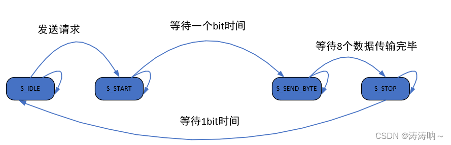
Block diagram of the receiving module:
module uart_rx
#(
	parameter	CLK_FRE	=	50,
	parameter	BAUD_RATE = 115200
)
(
	input				clk,
	input				rst,
	input				rx_pin,
	input				rx_ready,

	output	reg		rx_valid,
	output	reg[7:0]	rx_data
	);

localparam	CYCLE = (CLK_FRE * 1000000)/BAUD_RATE;

localparam	S_IDLE 		= 0;
localparam	S_START		= 1;
localparam	S_RX_CYCLE 	= 2;
localparam	S_DATA		= 3;
localparam	S_STOP 		= 4;

reg[2:0]		state;
reg[2:0]		next_state;
reg			rx_d0;
reg			rx_d1;
wire			rx_negedge;
reg[7:0]		rx_bits;
reg[2:0]		bit_cnt;
reg[15:0]	cycle_cnt;

assign	rx_negedge = ~rx_d0 && rx_d1;
//Message frame start bit,下降沿
[email protected](posedge clk or negedge rst)
begin
if(rst == 1'b0)
	begin
	rx_d0 <= 1'b0;
	rx_d1 <= 1'b0;
	end
else
	begin
	rx_d0 <= rx_pin;
	rx_d1 <= rx_d0;
	end
end

[email protected](posedge clk or negedge rst)
begin
if(rst == 1'b0)
	state <= S_IDLE;
else
	state <= next_state;
end
//状态转移
[email protected](*)
begin
	case(state)
		S_IDLE:
			if(rx_negedge)
				next_state <= S_START;
			else
				next_state <= S_IDLE;
		S_START:
			if(cycle_cnt == CYCLE-1)
				next_state <= S_RX_CYCLE;
			else
				next_state <= S_START;
		S_RX_CYCLE:
			if(cycle_cnt == CYCLE-1 && bit_cnt == 3'd7)
				next_state <= S_STOP;
			else
				next_state <= S_RX_CYCLE;
		S_STOP:
			if(cycle_cnt == CYCLE/2-1)
				next_state <= S_DATA;
			else
				next_state <= S_STOP;
		S_DATA:
			if(rx_ready)
				next_state <= S_IDLE;
			else
				next_state <= S_DATA;
		default:
			next_state <= S_IDLE;
	endcase
end
//波特率计数器
[email protected](posedge clk or negedge rst)
begin
if(rst == 1'b0)
	cycle_cnt <= 16'd0;
else if((state == S_RX_CYCLE && cycle_cnt == CYCLE-1)||next_state != state)
	cycle_cnt <= 16'd0;
else
	cycle_cnt <= cycle_cnt + 16'd1;
end
//Bit counter
[email protected](posedge clk or negedge rst)
begin
if(rst == 1'b0)
	bit_cnt <= 3'd0;
else if(state == S_RX_CYCLE )
	if(cycle_cnt == CYCLE-1)
		bit_cnt <= bit_cnt + 3'd1;
	else
		bit_cnt <= bit_cnt;
else
	bit_cnt <= 3'd0;
end
//Serial data is converted to parallel data
[email protected](posedge clk or negedge rst)
begin
if(rst == 1'b0)
	rx_bits <= 8'd0;
else if(state == S_RX_CYCLE && cycle_cnt == CYCLE/2-1)
	rx_bits[bit_cnt] <= rx_pin;
else
	rx_bits <= rx_bits;
end
//Data reception valid flag
[email protected](posedge clk or negedge rst)
begin
if(rst == 1'b0)
	rx_valid <= 1'b0;
else if(state == S_STOP && next_state != state)
	rx_valid <= 1'b1;
else if(state == S_DATA && rx_ready)
	rx_valid <= 1'b0;
end
//数据接收
[email protected](posedge clk or negedge rst)
begin
if(rst == 1'b0)
	rx_data <= 8'd0;
else if(state == S_STOP && next_state != state)
	rx_data <= rx_bits;
else
	rx_data <= rx_data;
end

endmodule
modelsim仿真
The overall waveform of the module is shown below
Two registers are used,Take advantage of non-blocking assignments,Take a pat on the input data,Then get the falling edge of the message frame.如下图所示:
The waveform diagrams of internal state transitions and registers are shown below:
3.顶层模块
Design a top-level program,让FPGA每隔1Send a string in seconds,And in the waiting time can receive the data sent by the computer,and send the received data toPC端.
The block diagram of the structure is shown below:
FPGARight every time data is receivedLED进行电平翻转,所以增加了LED输出口,控制LED0.
代码如下:
module uart_test
#(
	parameter		CLK_FRE = 50,
	parameter		BAUD_RATE = 115200
)
(
	input		clk,
	input		rst,
	input		rx,
	output	tx,
	output reg	led
	);

localparam		IDLE = 0;
localparam		SEND = 1;
localparam		WAIT = 2;

reg[1:0]		state;
reg[1:0]		next_state;

reg[7:0]		tx_data;
reg[7:0]		tx_str;
reg				tx_data_valid;
wire			tx_data_ready;

wire				rx_ready;
wire[7:0]		rx_data;
wire			rx_valid;

reg[3:0]		tx_cnt;
reg[31:0]		wait_cnt;

assign rx_ready = 1'b1;

[email protected](posedge clk or negedge rst)
begin
	if(rst == 1'b0)
		begin
			wait_cnt <= 32'd0;
			tx_cnt <= 8'd0;
			state <= IDLE;
			tx_data <= 8'd0;
			tx_data_valid <= 1'b0;
			led <= 1'b0;
		end
	else
		case(state)
			IDLE:
				state <= SEND;
			SEND:
				begin
					wait_cnt <= 32'd0;
					tx_data <= tx_str;
					if(tx_data_valid == 1'b1 && tx_data_ready == 1'b1 && tx_cnt < 4'd12)//发送字符串"I LOVE YOU"
					begin
						tx_cnt <= tx_cnt + 4'd1;
					end
					else if(tx_data_valid && tx_data_ready)//Wait for the last byte to be sent
					begin
						tx_cnt <= 8'd0;
						tx_data_valid <= 1'b0;
						state <= WAIT;
					end
					else if(~tx_data_valid)
					begin
						tx_data_valid <= 1'b1;
					end
				end
			WAIT://等待1s的间隔,The string can be received during the waiting time,and sent to the sending module
			begin
				wait_cnt <= wait_cnt +1'b1;
				if(rx_valid == 1'b1)
				begin
					tx_data_valid <= 1'b1;
					tx_data <= rx_data;
					led <= ~led;
				end
				else if(tx_data_valid && tx_data_ready)
				begin
					tx_data_valid <= 1'b0;
				end
				else if(wait_cnt >= CLK_FRE * 1000000)
				begin
					state <= SEND;
				end
			end
			default:
					state <= IDLE;
		endcase
	end
//要发送的字符串
[email protected](*)
begin
	case(tx_cnt)
	4'd0:tx_str <= "I";
	4'd1:tx_str <= " ";
	4'd2:tx_str <= "L";
	4'd3:tx_str <= "O";
	4'd4:tx_str <= "V";
	4'd5:tx_str <= "E";
	4'd6:tx_str <= " ";
	4'd7:tx_str <= "Y";
	4'd8:tx_str <= "O";
	4'd9:tx_str <= "U";
	4'd10:tx_str <= "\r";
	4'd11:tx_str <= "\n";
	default:tx_str <= 8'd0;
	endcase
end

uart_tx
#(
		.CLK_FRE	(CLK_FRE),
		.BAUD_RATE	(BAUD_RATE)
)uart_tx
(
	.clk(clk),
	.rst(rst),
	.tx_data(tx_data),
	.tx_data_valid(tx_data_valid),

	.tx_pin(tx),
	.tx_data_ready(tx_data_ready)
);

uart_rx
#(
	.CLK_FRE	(CLK_FRE),
	.BAUD_RATE 	(BAUD_RATE)
)uart_rx
(
	.clk(clk),
	.rst(rst),
	.rx_pin(rx),
	.rx_ready(rx_ready),

	.rx_valid(rx_valid),
	.rx_data(rx_data)
	);

endmodule
四、实验结果
使用UCF文件对FPGA端口进行定义:
NET "clk" LOC = T8 | TNM_NET = sys_clk_pin;
TIMESPEC TS_sys_clk_pin = PERIOD sys_clk_pin 50000 kHz;

##
NET "rst"                  LOC = L3 | IOSTANDARD = "LVCMOS33";         ## reset pushbutton

##################################################################################
#USB Serial RS232 Pin define
##################################################################################
NET "rx"                LOC = C11 | IOSTANDARD = "LVCMOS33";   	## Uart RXD:U4_TXD
NET "tx"                LOC = D12 | IOSTANDARD = "LVCMOS33"; 	## Uart TXD:U4_RXD
##################################################################################
#LED Pin define
##################################################################################
NET "led"               LOC = P4 | IOSTANDARD = "LVCMOS33";       ## LED1
1、代码调试
1、ERROR:HDLCompiler:1511 - “C:\Users\HP\Desktop\FPGA_demo\04_uart\rtl\uart_rx.v” Line 29: Mix of blocking and non-blocking assignments to variable <rx_bits> is not a recommended coding practice.
错误原因:Blocking assignment is used at the same time as non-blocking assignment
2、Latch Warning,caseStatements need to be written in full,一定要写”default“,Responsible will generate unwanted latches,It will affect the subsequent timing design.The defined register must be given an initial value,Responsible also generates latches.
2、实验结果
The serial port result is shown in the figure:
边栏推荐
- Mysql database installation and configuration detailed tutorial
- std::format格式化自定义类型
- Construction inspection, no rules and no square
- 22/8/9 Collection of Greedy Problems
- Engineering Design of Single-sided PCB Routing Impedance
- 22/8/9 贪心问题合集
- MySQL advanced query
- Successfully resolved TypeError: can't multiply sequence by non-int of type 'float'
- Shell编程三剑客之sed
- 络达开发---自定义BLE服务(二):功能实现
猜你喜欢

ABP中的数据过滤器

R语言多元线性回归、ARIMA分析美国不同候选人对经济GDP时间序列影响

Dual machine thermal for comprehensive experiment (VRRP + OSPF + + NAT + DHCP + VTP PVSTP + single-arm routing)

paddle2.3和torch1.8在SentenceBert上的性能对比
![[Server data recovery] Data recovery case of lvm information and VXFS file system corruption caused by raid5 crash](/img/dc/043f861507fc16530446bf051941ef.jpg)
[Server data recovery] Data recovery case of lvm information and VXFS file system corruption caused by raid5 crash

2022年PMP报考指南

简陋的nuxt3学习笔记

Lianshengde W801 series 6-Analyze the Bluetooth communication source code of W801 from the perspective of WeChat applet (indicate method)

【微波工程学习记录1】功率分配器和定向耦合器

二维数组实战项目--------《扫雷游戏》
随机推荐
Data Filters in ABP
进程间通信方式(2)有名管道
【Video】Report Sharing | 2021 Insurance Industry Digital Insights
The SAP ABAP JSON format data processing
postgresql参数意义
Still using Xshell?You are out, recommend a more modern terminal connection tool, easy to use!
Shell 文本三剑客 Sed
版本号大小的判断方法
软件测试面试题:I P协议、RARP协议、ICMP协议与ARP协议的功能是什么?
生信实验记录(part2)--tf.reduce_sum()用法介绍
HCIP-R&S By Wakin自用笔记(3)OSPF之引入外部路由、Forwarding-Address、汇总、特殊区域
Two-dimensional array combat project -------- "Minesweeper Game"
Data Analysis Interview Manual "SQL"
Ambari迁移Spark2到其它机器(图文教程)
Ambari Migrates Spark2 to Other Machines (Graphic and Text Tutorial)
生信实验记录(part3)--scipy.spatial.distance_matrix
二维数组实战项目--------《扫雷游戏》
16. 最接近的三数之和
16. Sum of the nearest three numbers
迭代器和生成器