当前位置:网站首页>3、 6 [Verilog HDL] gate level modeling of basic knowledge
3、 6 [Verilog HDL] gate level modeling of basic knowledge
2022-04-23 09:12:00 【FPGA Bridge】
Reference books :《Verilog HDL Digital design and synthesis 》 The second edition , This document is the third 5 Study notes for . Because this chapter also describes the modeling method . This modeling method is the bottom abstraction level commonly used by designers . The lower level is switch level modeling .
To learn more about switch level modeling of low-level modeling :
Introduction to basic digital and electrical knowledge of gate circuit , Please refer to my relevant 《 Fundamentals of digital electronic technology 》 Books, reading notes , It is helpful for everyone to have an in-depth understanding and learning of gate level modeling
 https://blog.csdn.net/arm_qiao/category_11744079.html
Learning goals
- master Verilog Provided gate level primitives
- Understand the application of doors
- Can write according to the gate circuit Verilog describe
- Clear the rise in door level design 、 Descent and shutdown delay
- Minimum in door level design 、 Maximum and typical delays
5.1 The type of door
The basic logic gates fall into two categories :1、 And / Or category (and/or);2、 Buffer / Non category (buf/not)
5.1.1 And gate (and) And or door (or)


The corresponding keywords are
and   // And gate            nand    // NAND gate
or    // Or gate            nor     // Or not
xor   // Exclusive OR gate          xnor    // xnor
When a gate level primitive instantiates a reference , We can not specify the name of the specific instance .
Door level instance reference :
wire OUT, IN1, IN2;

// Instance reference of basic door
and   a1(OUT, IN1, IN2);
nand  na1(OUT, IN1, IN2);
or    or1(OUT, IN1, IN2);
nor   nor1(OUT, IN1, IN2);
xor   xor1(OUT, IN1, IN2);
xnor  xnor1(OUT, IN1, IN2);
// There are more than two inputs ; Three input NAND gate
nand na1_3inp(OUT, IN1, IN2, IN3);
5.1.2 Buffer / Not gate (buf/not)


Corresponding keywords , And keyword instance references
// keyword
buf    // Buffer           not      // Not gate
// Buffer door 、 Call of non gate   , Instance reference can be done without instance naming
buf b1(OUT1, IN);
not n1(OUT1, IN);

// There are more than two outputs
buf b1_2out(OUT1, OUT2, IN);
Buffer with control end / Not gate (bufif / notif)
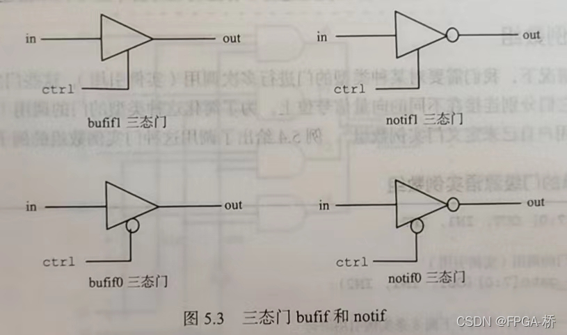

Corresponding keywords , And keyword instance references
// keyword
bufif1   // High level enable on buffer gate       notif1      // High level enable non gate
bufif0   // Low level enable on buffer gate       nitif0      // Low level non conducting gate
// Instantiate reference
bufif1 b1(out, in ,ctrl);
bufif0 b0(out, in ,ctrl);

notif1 n1(out, in, ctrl);
notif0 n0(out, in, ctrl);
5.1.3 Instance array
There are many cases , Multiple calls to the same door type are required ( Instance reference ), The only difference between these same gate instances is that they are connected to different vector signal bits , To simplify this type of door ,Verilog Allow the user to define the door instance array .
// Simple gate level primitive instance array
wire [3:0] OUT, IN1, IN2;       // The statement 3 individual 4 Bitline variable

// Array call of basic gate
nand n_gate[3:0] (OUT, IN1, IN2);

// The above statement is equivalent to 4 Instance reference statement
nand n_gate0(OUT[0], IN1[0], IN2[0]);
nand n_gate1(OUT[1], IN1[1], IN2[1]);
nand n_gate2(OUT[2], IN1[2], IN2[2]);
nand n_gate3(OUT[3], IN1[3], IN2[3]);
5.1.4 Door level modeling example
(1) Gate multiplexer

Pin information table and function truth table
| Input / output signal description | |||
| The signal | A wide | type | Function description |
| i0 | 1bit | input | Input signal 0 |
| i1 | 1bit | input | Input signal 1 |
| i2 | 1bit | input | Input signal 2 |
| i3 | 1bit | input | Input signal 3 |
| s0 | 1bit | input | Address input signal |
| s1 | 1bit | input | Address input signal |
| out | 1bit | output | The output signal |
| mux_4_1 Data selector truth table | |||
| Input signal | Address input signal | Output | |
| s0 | s1 | out | |
| i0 | 0 | 0 | i0 |
| i1 | 0 | 1 | i1 |
| i2 | 1 | 0 | i2 |
| i3 | 1 | 1 | i3 |
Block
module mux_4_1(out, i0, i1, i2, i3, s1, s0);
// Input / output port declaration of the module
    output out;
    input i0, i1, i2, i3;
    input s1, s0;

// Module internal network connection variable declaration
    wire s1n, s0n;
    wire y0, y1, y2, y3;

// Not gate (not) Instance reference
    not n1(s1n, s1);
    not n0(s0n, s0);
// And gate (and) Instance reference
    and a0(y0, i0, s1n, s0n);
    and a1(y1, i1, s1n, s0);
    and a2(y2, i2, s1,  s0n);
    and a3(y3, i3, s1,  s0);
// Or gate (or) Instantiate reference
    or (out, y0, y1, y2, y3);
endmodule
After logic synthesis of program block RTL Logic diagram :

because RTL There are no three wire and gates and four wire or gates . Therefore, two two-wire and gates are used to replace one and gate of three wires ; Replace a four wire and gate with three two wire or gates , At the same time, the not gate here is directly added to the pin of and gate and or gate . The above figure is synthesized through logic RTL Comparing the logic diagram with the original logic selector, it is found that there is no logic error .
Excitation block
module tb_mux_4_1();
// Declare the connection variable between the excitation block and the code block
    wire OUT;
    reg IN0, IN1, IN2, IN3;
    reg S1, S0;
// Instance references a code block and connects variables
    mux_4_1  mux_4_1_stim(OUT, IN0, IN1, IN2, IN3, S1, S0);

    initial begin
        IN0 = 1'b1;  IN1 = 1'b0;  IN2 = 1'b1;  IN3 = 1'b0;
        #30 $display("IN0=%b, IN1=%b, IN2=%b, IN3=#b\n", IN0, IN1, IN2, IN3);
        // choice IN0
        S1 = 0;  S0 = 0;
        #30 $display("s1=%b, s0=%b, OUT=%b\n", S1, S0, OUT);
        // choice IN1
        S1 = 0;  S0 = 1;
        #30 $display("s1=%b, s0=%b, OUT=%b\n", S1, S0, OUT);
        // choice IN2
        S1 = 1;  S0 = 0;
        #30 $display("s1=%b, s0=%b, OUT=%b\n", S1, S0, OUT);
        // choice IN3
        S1 = 1;  S0 = 1;
        #30 $display("s1=%b, s0=%b, OUT=%b\n", S1, S0, OUT);
    end
endmodule
The logic simulation results are obtained through logic simulation , There is no error in comparing with the truth table .

(2) Four bit pulse carry full adder
The four bit pulse carry adder can be composed of four one bit full adders .

One bit full adder can be composed of two one bit half adders , Add the same or gate to form .
One bit full adder logic :
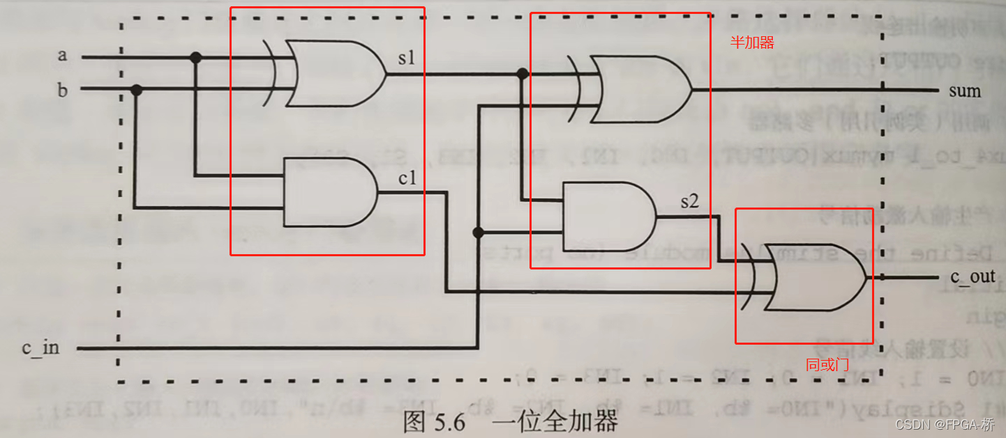
Code block
// One bit adder
module full_add(sum, c_out, a, b, c_in);
// Port variable declaration
    output sum, c_out;
    input  a, b, c_in;
// Intranet cable variable declaration
    wire s1, c1, s2;

// Gate level instantiation
    xor (s1, a, b);
    and (c1, a, b);

    xor (sum, s1, c_in);
    and (s2, s1, c_in);

    xor (c_out, s2, c1);
endmodule
Make a comprehensive analysis of it , You can see RTL Logical view , And compare it with its logic schematic diagram :

// Four bit pulse carry full adder , For the top-level module
module full_add4(sum, c_out, a, b, c_in);
// Port variable declaration
    output [3:0] sum;
    output c_out;
    input [3:0] a, b;
    input c_in;
// Intranet variable declaration
    wire c1, c2, c3;
// Instantiate the full adder , Connect in series to form 4 Bit pulse full adder
    full_add fa0(sum[0], c1, a[0], b[0], c_in);
    full_add fa1(sum[1], c2, a[1], b[1], c1);
    full_add fa2(sum[2], c3, a[2], b[2], c2);
    full_add fa3(sum[3], c_out, a[3], b[3], c3);
endmodule
It is logically synthesized to generate RTL Logical view , Compared with its principle logic view, we can see , No problem :

Excitation block : Verify the logical function of the code block
// Logic simulation excitation block
//Company:  Chaser —— The small workshop of the bridge
module tb_full_add4();
    reg [3:0] A, B;
    reg C_IN;
    wire [3:0] SUM;
    wire C_OUT;

// Instantiation
    full_add4 fadd4(SUM, C_OUT, A, B, C_IN);

    initial begin
        $monitor($time, "A=%b, B=%b, C_IN=%b, -----  C_OUT=%b, SUM=%b\n", A, B, C_IN, C_OUT, SUM);
    end
    initial begin
        A = 4'd0;   B = 4'd0;  C_IN = 1'b0;
        #50 A = 4'd3;   B = 4'd4;
        #50 A = 4'd2;   B = 4'd5;
        #50 A = 4'd9;   B = 4'd9;
        #50 A = 4'd10;   B = 4'd15;
        #50 A = 4'd10;   B = 4'd5;  C_IN = 1'b1;
    end
endmodule
The simulation results are shown in the figure below :

5.2 Gate delay
stay MOS In the circuit composed of tubes, it is formed due to the internal equivalent capacitance and resistance RC circuit , Therefore, in 0、1 When the change , There must be a change delay , If you can't understand this sentence , Please be sure to relearn CMOS Gate circuit . This chapter is only a brief introduction to delay , More detailed explanation , It will be explained and learned in Chapter 10 .
5.2.1 rising 、 Descent and shutdown delay
stay Verilog In gate level primitives , There are three kinds of delay from input to output .
-
Rise delay
When the input of the door changes , The output of the door is from 0,X,Z Change to 1 The time required is called the rise delay .

-
Descent delay
The descent delay is the input of the gate from 1,X,Z Change to 0 Time required

- Shutdown delay
Turn off delay refers to the output of the gate from 0,1,X, Change to high impedance Z Time required .
in addition , If the value changes to an uncertain value X, Then the required time can be regarded as the one with the smallest delay value of the above three types .
stay Verilog in , The user can use three different methods to explain the delay of the door .
- When a delay value is specified , This value is used for all delay types
- When two delay values are specified , Represents rise delay and fall delay respectively
- When three delay values are specified , Respectively represents the rise delay 、 Descent delay and shutdown delay
- If no delay time is specified , Then the default delay value is 0
// Gate delay value description
// A delay value
and #(delay_time) a1(out, i1, i2);
and #(5) a11(out, i1, i2);
// Two delay values
and #(rise_val, fall_val) a2(out, i1, i2);
and #(4, 6)  a21(out, i1, i2);
// Three delay values
bufif0 #(rise_val, fall_val, turnoff_val) b1(out, in, control);
bufif0 #(3, 4, 5) b11(out, in, cintrol);
5.2.2 Minimum 、 classic 、 Maximum delay
stay Verilog in , In addition to specifying the above three delays , For each type of delay, you can also specify its minimum value 、 Maximum and typical delay . It can be specified at the beginning of the simulation , You can also specify during the simulation . The specific control method is related to the simulator and operating system used , If not specified, it defaults to the typical delay value .
Verilog Users can flexibly respond to various types of delays in the design ( rising 、 falling 、 A typical ) Use three different specific values , The delay value can be used for simulation without modifying the design .
// A delay
// Minimum delay =4
// Typical delay =5
// Maximum delay =6
and #(4:5:6) a1(out, i1, i2);

// Two delays
// Minimum delay , Rise delay =3, Descent delay =5, Shutdown delay =min(3,5)
// Typical delay , Rise delay =4, Descent delay =6, Shutdown delay =min(4,6)
// Maximum delay , Rise delay =5, Descent delay =7, Shutdown delay =min(5,7)
and #(3:4:5, 5:6:7) a2(out, i1, i2);

// Three delays
// Minimum delay , Rise delay =3, Descent delay =5, Shutdown delay =7
// Typical delay , Rise delay =4, Descent delay =6, Shutdown delay =8
// Maximum delay , Rise delay =5, Descent delay =7, Shutdown delay =9
and #(3:4:5, 5:6:7, 7:8:9) a3(out, i1, i2);


// From the command line, you can start the line mode
> verilog test.v +maxdelays
5.2.3 Examples of delays
module delay(out, a, b, c);
    output out;
    input a,b,c;
    wire e;
    and #(50) a1(e,a,b);
    or #(40) o1(out,e,c);
endmodule
module tb_delay();
wire OUT;
reg A,B,C;
delay d1(OUT,A,B,C);
initial begin
A=1'b0; B=1'b0; C=1'b0;
#100 A=1'b1; B=1'b1; C=1'b1;
#100 A=1'b1; B=1'b0; C=1'b0;
#200 $finish;
end
endmodule
版权声明
本文为[FPGA Bridge]所创,转载请带上原文链接,感谢
https://yzsam.com/2022/04/202204230911010324.html
边栏推荐
- Group Backpack
- SAP 101K 411K 库存变化
- Valgrind et kcachegrind utilisent l'analyse d'exécution
- How to read excel table to database
- Principle of synchronized implementation
- Program, process, thread; Memory structure diagram; Thread creation and startup; Common methods of thread
- Brief steps to build a website / application using flash and H5
- Failed to download esp32 program, prompting timeout
- 调包求得每个样本的k个邻居
- Kettle实验 转换案例
猜你喜欢

SAP 101K 411k inventory change

Correct method of calculating inference time of neural network

Bk3633 specification

資源打包關系依賴樹

PLC point table (register address and point table definition) cracking detection scheme -- convenient for industrial Internet data acquisition

Summary of solid problems

PCTP考试经验分享

搞不懂时间、时间戳、时区,快来看这篇

What is monitoring intelligent playback and how to use intelligent playback to query video recording

2022-04-22 openebs cloud native storage
随机推荐
Open services in the bottom bar of idea
MySQL小練習(僅適合初學者,非初學者勿進)
[SQL Server fast track] view and cursor of database
Get trustedinstaller permission
Initial experience of talent plan learning camp: communication + adhering to the only way to learn open source collaborative courses
NPM reports an error: operation not allowed, MKDIR 'C: \ program files \ node JS \ node_ cache _ cacache’
Non duplicate data values of two MySQL query tables
Error: cannot find or load main class
I don't understand time, timestamp and time zone. Look at this article
MYCAT configuration
Failed to download esp32 program, prompting timeout
Image processing in opencv -- Introduction to contour + contour features
L2-024 部落 (25 分)(并查集)
What is monitoring intelligent playback and how to use intelligent playback to query video recording
Program, process, thread; Memory structure diagram; Thread creation and startup; Common methods of thread
爬虫使用xpath解析时返回为空,获取不到相应的元素的原因和解决办法
npm ERR! network
L2-024 tribe (25 points) (and check the collection)
ALV树(LL LR RL RR)插入删除
搞不懂时间、时间戳、时区,快来看这篇