当前位置:网站首页>Data storage implementation of SDRAM and read and write operations on its data
Data storage implementation of SDRAM and read and write operations on its data
2022-08-09 07:32:00 【an-ning】
SDRAMOn realization of data storage and the data read and write operations
文章目录
1 SDRAM
1.1 简介
SDRAM(Synchronous Dynamic Random Access Memory),The synchronous dynamic random access memory.同步是指内存工作需要同步时钟,Internal commands and data transmission for sending it as benchmark;The dynamic is refers to the storage array need to constantly refresh to ensure that data is not lost;According to random index is not stored in order,And random specified address for data read and write operations.SDARMReading and writing is a complex process,Line including activated、Column, speaking, reading and writing、预充电、Refresh and a series of operation.
1.2 SDRAM结构和原理
1、结构:
![[外链图片转存失败,源站可能有防盗链机制,建议将图片保存下来直接上传(img-DdQaYTvm-1659576614933)(SDRAMOn realization of data storage and the data read and write operations.assets/1658315590878.png)]](/img/a4/61895f994939cdd6f069300276fd7b.png)
SDRAM的内部是一个存储阵列,We think it can be as a table
2、原理:When to write data in the table,Need to specify line(Row),再指定列(Column),就可以准确地找到所需要的“单元格”.SDRAMStoring data is to use the charge and discharge characteristic of the capacitance and the ability to maintain the ability to charge.一个大小为1bitThe structure of the storage unit as shown in the figure below:
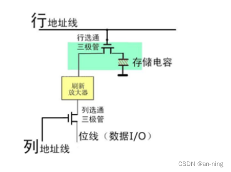
It is mainly composed of ranks of strobe triode,Storage capacity,Refresh an amplifier.行地址与列地址选通使得Storage capacity与数据线导通,从而可进行放电(读取)与充电(写入)操作.
3、特点:SDRAM具有空间存储量大、读写速度快、价格相对便宜等优点.然而由于SDRAM内部利用电容来存储数据,为保证数据不丢失,需要持续对各Storage capacity进行刷新操作;同时在读写过程中需要考虑行列管理、各种操作延时等,由此导致了其控制逻辑复杂的特点.
1.3 SDRAM块
1、“单元格”就是SDRAMMemory chips in the storage unit,而这个“表格”(存储阵列)我们称之为L-Bank.通常SDRAM的存储空间被划分为4个L-Bank,在寻址时需要先指定其中一个L-Bank,然后在这个选定的L-Bank中选择相应的行与列进行寻址(寻址就是指定存储单元地址的过程).
2、容量计算:
对SDRAMRead and write is in view of the storage unit for,对SDRAMFor a storage unit of capacity equal to the data bus bits wide,单位是bit.那么SDRAMChip, the total storage capacity, we can through the following formula calculated:
SDRAM总存储容量 = L-Bank的数量×行数×列数×存储单元的容量(Of the data line)
2 SDRAM的操作
2.1 SDRAMThe chip initialization
SDRAMChip after electricity needs an initialization process,To guarantee the normal work of the chip can according to the expected way,The initialization process is shown in figure
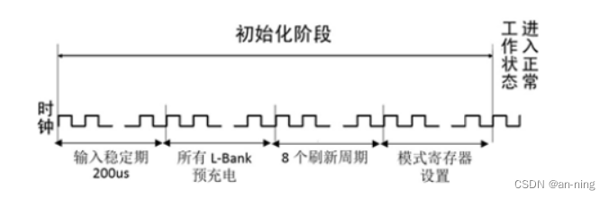
SDRAMAfter the electricity to have200usThe input to the plateau,In this period of time can't forSDRAMThe interface to do any operation; 200usAfter allL-Bank预充电,然后是连续8次刷新操作;The last set mode register.Initialize the key stage is the mode register(MR,Mode Register)的设置,简MRS(MR Set),Mode register set is mainly used to determine the chip works,Including the burst length(Burst Length)、潜伏期(CAS Latency)As well as the operation mode, etc.
2.2 SDRAM行激活
初始化完成后,无论是读操作还是写操作,都要先激活(Active)SDRAM中的一行,To make it active(Line is also called the effective).Before this will goSDRAMThe chip selection andL-Bank的定址,But they and activation can be simultaneously.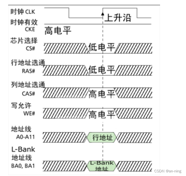
从上图可以看出,在片选CS#(#表示低电平有效)、L-BankAddressing at the same time,RAS(Row Address Strobe,Row address strobe pulse 冲)也In the effective状态.此时AnAddress line, send a specific address.如图中是A0- A11,共有12个地址线,Because it is a binary representation, 所以共有4096个行(2^12=4096),A0-A11The different values will determine the specific address.Because the line activation as well as the correspondingL-Bank有效,So line activation can also be calledL-Bank有效.
2.3 SDRAMColumn, speaking, reading and writing
Line after activation address,就要对列地址进行寻址了.由于在SDRAM中,Address line is Shared by line,Therefore columns addressing the address line is stillA0-A11.在寻址时,利用RAS(Row Address Strobe,Row address strobe pulse冲)与CAS(Column Address Strobe,列地址选通脉冲)Addressing to district branch with columns addressing,如图所示.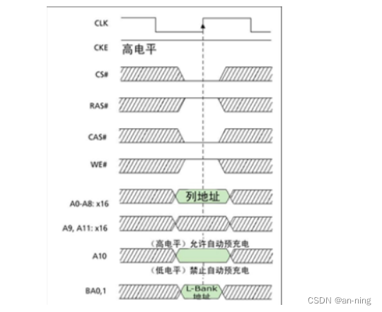
图中“x16”Said storage unit capacity of16bit.一般来说,在SDRAMStored in the array(L-Bank) The number of columns of less than the number of lines,The column address a width less than the line,So when the row address strobe address line high may not use.
2.4 数据输入输出
1、数据输出(即读操作):在选定列地址后,就已经确定了具体的存储单元,The rest of the things is data through dataI/O通道(DQ)输出到内存总线上了.但是在CAS发出之后,仍要经过一定的时间才能有数据输出,从CASWith the read command issued to first Pen data output this time,被定义为CL(CAS Latency,CAS潜伏期).CL时间越短,读数据时SDRAMThe faster response.由于CL只在读取时出现,所以CLIncubation period is also known as read(RL,Read Latency).CLUnits withtRCD一样,为时钟周期数,Specific time is determined by the clock frequency.
2、数据输入(即写操作):数据写入的操作也是在tRCD之后进行,But at the moment, noCL(记住,CL只出现在读取操作中),Send data and written instructions at the same time.不过,Data does not write storage unit in real time,The real write data needs certain cycle.In order to ensure reliable data to write,Will set aside enough to write/校正时间(tWR, Write Recovery Time),This operation is also known as write back(Write Back).tWRTake at least one clock cycle or a little more(时钟频率越高,tWRTake up the more cycles)
2.5 突发长度
1、突发长度:
突发(Burst)是指在同一行中相邻的存储单元连续进行数据传输的方式,连续传输所涉及到存储单元(列)的数量就是突发长度(Burst Lengths,简称BL).
2、读/写操作,都是一次对一个存储单元进行寻址.However in reality rarely only forSDRAM In a single storage space to read and write,Usually need to complete the continuous transmission of data in storage.在连续读/写操作时,In order to a unit under the current storage unit for addressing,Need to keep sending column address and read/写命令(行地址不变,所以不用再对行寻址).
2.6 预充电
1、预充电:在对SDRAM某一存储地址进行读写操作结束后,如果要对同一L-Bank的另一行进行寻址, 就要将原来有效(工作)的行关闭,重新发送行/列地址.L-Bank关闭现有工作行,准备打开新行的操作就是预充电(Precharge).
在读写过程中,工作行内的存储体由于“行激活”而使Storage capacity受到干扰,因此在关闭工作行前需要对本行所有存储体进行重写.预充电实际上就是对工作行中所有存储体进行数据重写,并对行地址进行复位,以准备新行工作的过程. Can charge in advance through the command control,Also can let chip through assisted set in advance after every read and write operations, automatically recharge.Now when we look back read and write operations command sequence diagram,We can find the address lineA10 Controls whether after reading and writing of the currentL-BankAutomatic charging in advance,这就是上文所说的“Auxiliary set”.And in a separate charge in the command,A10Is controlled to specifiedL-Bank还是所有的L-Bank(当有多个L-BankIn the effective/Active)进行预充电,The former needs to provideL-Bank的地址,The latter simplyA10The signal in a high level.在发出预充电命令之后,After a period of time to send off the activation command to open the new working line,这个间隔被称为tRP(Precharge command Period,预充电有效周期),和tRCD、CL一样,tRPNumber of units is also a clock cycle,The specific value depending on the clock frequency.Read the preliminary charging sequence diagram(CL=2、BL=4、tRP=2)写操作时,Due to the real data every writing requires a cycle to ensure that enough,This period of time is to write cycle back(tWR).So can't write with pre charging operation at the same time,必须要在tWRCommand signal charge only after,In order to ensure reliable data to write,Or rewrite the data might be wrong .
2.7 刷新
1、SDRAM之所以称为同步“动态”随机存储器,就是因为它要不断进行刷新(Refresh)才能保留住数据,因此刷新是SDRAM最重要的操作.Refresh operation is similar to pre charge,Are rewrite the data in memory.But why are charging operation to refresh?Because in one or all of the charge is onL-BankLine of work(Active line)操作,And are not on a regular basis;The refresh is a fixed cycle,And so on all lines operation,To keep those for a long time didn't experience to rewrite the data in a storage body.但与所有L-BankPre charge is different,In this case, the line is allL-BankAddress is the same 行,And in the pre chargeL-BankIn the work line is not address must be the same.
2、目前公认的标准是,存储体中电容的数据有效保存期上限是64ms,也就是说每一行刷新的循环周期是64ms.我们在看SDRAM芯片参数时,经常会看到4096 Refresh Cycles/64ms或8192 Refresh Cycles/64ms的标识,这里的4096与8192就代表这个芯片中每个L-Bank的行数.刷新命令一次仅对一行有效,也就是说在64msIn this two specifications of the chip needs to be done4096次和8192次刷新操作.因此,L-Bank为4096During the refresh command sending interval for 15.625μs(64ms/4096),8192行时为7.8125μs(64ms/8192).
3 基于SDRAMThe data read and write
3.1 主要实现过程
1、思想:
PCMachine via a serial port to theSDRAMWrite data chip breaking,Through the buttons initiate read requests,Will be written to the data of sudden read,And once again via a serial port back toPC端.SDRAMAfter power on has reached the awaited state waiting for200us,200us之后对所有L-BankPre charge processing,After charging automatically refresh(一般持续8个周期),Then register the mode initialization Settings,主要设置SDRAM的突发长度、The incubation period and the operation mode, etc,至此sdram的初始化就完成了.sdram进入空闲状态,When you have to read and write requirements,sdramAdvanced line activation operation,Then according to the command column, speaking, reading and writing,When after the completion of the sudden, speaking, reading and writing are pre charge again,And then back to idle waiting for,If need to refresh automatically at this time,Send an automatic refresh command and enter automatically refresh the status,After the completion of the refresh again return to the idle state.状态图如下: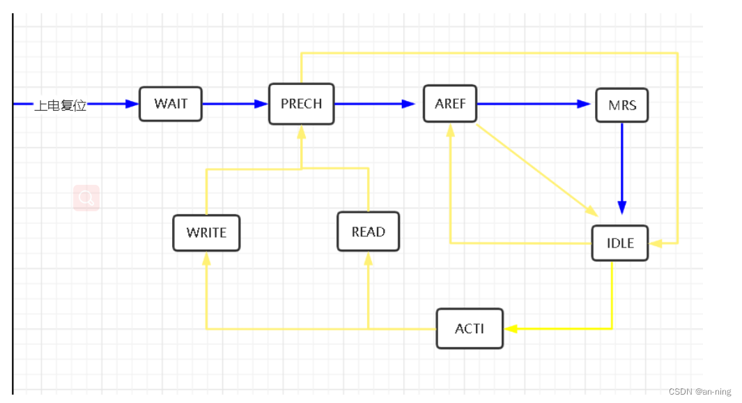
2、由于SDRAMThe various states of operation is complicated,而Platform Designer提供的SDRAM IP The resolution of the nuclear interface greatly to ourSDRAM的使用,Therefore realize when we need to callIPNuclear to accomplish these complex operation,我们只需要在sdramControl module to complete due to read and write operations can be.
3、sdram控制模块代码
module sdram_ctrl (
    input            clk               ,                    //sdram时钟100MHz
    input            clk_in            ,                    //fifoThe data input clock50MHz
    input            clk_out           ,                    //fifoThe data output of the clock50MHz
    input            rst_n             ,                    //复位信号
    input   [7:0]    din               ,                    //写入数据,Put first to writefifo中
    input            din_vld           ,                    //
    input            rd_req            ,                    //读请求
    input            ready             ,                    //txSend signals to shake hands with
    output  [7:0]    dout              ,                    //读出的数据,由读fifo获取
    output           dout_vld          ,                    //

    output  [23:0]   avm_address       ,                    //sdram地址2位bank地址+13位行地址+9位列地址
    output  [15:0]   avm_writedata     ,                    //写数据,写fifo的输出
    output           avm_read          ,                    //读使能
    output           avm_write         ,                    //写使能
    input   [15:0]   avs_readdata      ,                    //读数据,To readfifo中
    input            avs_readdatavalid ,
    input            avs_waitrequest                        //
    );

//状态机参数定义
    parameter   IDLE  = 3'b001 ,                            //空闲状态
                WRITE = 3'b010 ,                            //写数据状态
                READ  = 3'b100 ;                            //读数据状态

//信号定义
    reg   [2:0]     cstate         ;
    reg   [2:0]     nstate         ;

    reg   [23:0]    cnt_wraddr     ;                        //Write the address counter
    wire            add_cnt_wraddr ;
    wire            end_cnt_wraddr ;

    reg   [23:0]    cnt_rdaddr     ;                        //Read the address counter
    wire            add_cnt_rdaddr ;
    wire            end_cnt_rdaddr ;

    reg   [7:0]     cnt_burst      ;                        //Read/write condition burst length counting
    wire            add_cnt_burst  ;
    wire            end_cnt_burst  ;

    reg             wr_flag        ;                        //写标志
    reg             rd_flag        ;                        //读标志
    reg             last_flag      ;                        //The last time to do
    reg             prior_flag     ;                        //Read and write priority judgment,高读低写

    reg   [7:0]     dout_r         ;
    reg             dout_r_vld     ;

    wire  [7:0]     wrfifo_data    ;
    wire            wrfifo_rdreq   ;
    wire            wrfifo_wrreq   ;
    wire  [15:0]    wrfifo_q       ;
    wire            wrfifo_empty   ;
    wire  [6:0]     wrfifo_usedw   ;
    wire            wrfifo_full    ;

    wire  [15:0]    rdfifo_data    ;
    wire            rdfifo_rdreq   ;
    wire            rdfifo_wrreq   ;
    wire  [7:0]     rdfifo_q       ;
    wire            rdfifo_empty   ;
    wire            rdfifo_full    ;

    wire            idle_to_write  ;
    wire            idle_to_read   ;
    wire            write_to_idle  ;
    wire            read_to_idle   ;

//The state machine transfer
    always @(posedge clk or negedge rst_n)
    begin
        if (!rst_n)
            cstate <= IDLE;
        else
            cstate <= nstate;
    end

    always @(*)
    begin
        case (cstate)
            IDLE:
            begin
                if (idle_to_write)
                    nstate = WRITE;
                else if (idle_to_read)
                    nstate = READ;
                else
                    nstate = cstate;
            end
            WRITE:
            begin
                if (write_to_idle)
                    nstate = IDLE;
                else
                    nstate = cstate;
            end
            READ:
            begin
                if (read_to_idle)
                    nstate = IDLE;
                else
                    nstate = cstate;
            end
            default:  ;
        endcase
    end

//The state machine transition conditions determine
    assign  idle_to_write = cstate == IDLE && (~prior_flag && wrfifo_usedw > `BURST_LEN) ;
    assign  idle_to_read  = cstate == IDLE && (rd_flag && prior_flag)                    ;
    assign  write_to_idle = cstate == WRITE && end_cnt_burst                             ;
    assign  read_to_idle  = cstate == READ && end_cnt_burst                              ;

/************************ 读写优先级仲裁 *************************/
    //wr_flag
    always @(posedge clk or negedge rst_n)
    begin
        if (!rst_n)
            wr_flag <= 0;
        else if (wrfifo_usedw > `BURST_LEN)
            wr_flag <= 1'b1;
        else
            wr_flag <= 1'b0;
    end

    //rd_flag
    always @(posedge clk or negedge rst_n)
    begin
        if (!rst_n)
            rd_flag <= 0;
        else if (~rd_flag && rd_req)
            rd_flag <= 1'b1;
        else if (rd_flag & idle_to_read)
            rd_flag <= 1'b0;
    end

    //last_flag
    always @(posedge clk or negedge rst_n)
    begin
        if (!rst_n)
            last_flag <= 0;
        else if (write_to_idle)
            last_flag <= 1'b0;
        else if (read_to_idle)
            last_flag <= 1'b1;
    end

    //prior_flag
    always @(posedge clk or negedge rst_n)
    begin
        if (!rst_n)
            prior_flag <= 0;
        else if (wr_flag && (last_flag || ~rd_flag))
            prior_flag <= 1'b0;
        else if (rd_flag && (~last_flag || ~wr_flag))
            prior_flag <= 1'b1;
    end

/****************************************************************/

//突发计数
    always @(posedge clk or negedge rst_n)
    begin
        if (!rst_n)
            cnt_burst <= 0;
        else if (add_cnt_burst)
        begin
            if (end_cnt_burst)
                cnt_burst <= 0;
            else
                cnt_burst <= cnt_burst + 1'b1;
        end
    end
    assign  add_cnt_burst = (cstate == WRITE || cstate == READ) && ~avs_waitrequest;
    assign  end_cnt_burst = add_cnt_burst && cnt_burst == `BURST_LEN - 1;

//Write the address counter
    always @(posedge clk or negedge rst_n)
    begin
        if (!rst_n)
            cnt_wraddr <= 0;
        else if (add_cnt_wraddr)
        begin
            if (end_cnt_wraddr)
                cnt_wraddr <= 0;
            else
                cnt_wraddr <= cnt_wraddr + 1'b1;
        end
    end
    assign  add_cnt_wraddr = cstate == WRITE && ~avs_waitrequest;
    assign  end_cnt_wraddr = add_cnt_wraddr && cnt_wraddr == `BURST_MAX - 1;

//Read the address counter
    always @(posedge clk or negedge rst_n)
    begin
        if (!rst_n)
            cnt_rdaddr <= 0;
        else if (add_cnt_rdaddr)
        begin
            if (end_cnt_rdaddr)
                cnt_rdaddr <= 0;
            else
                cnt_rdaddr <= cnt_rdaddr + 1'b1;
        end
    end
    assign  add_cnt_rdaddr = cstate == READ && ~avs_waitrequest;
    assign  end_cnt_rdaddr = add_cnt_rdaddr && cnt_rdaddr == `BURST_MAX - 1;

//dout_r
    always @(posedge clk_out or negedge rst_n)
    begin
        if (!rst_n)
        begin
            dout_r <= 0;
            dout_r_vld = 0;
        end
        begin
            dout_r <= rdfifo_q;
            dout_r_vld <= rdfifo_rdreq;
        end
    end

//例化写fifo
    wrfifo	            wrfifo_inst (
	.aclr               (~rst_n       ),
	.data               (wrfifo_data  ),
	.rdclk              (clk          ),
	.rdreq              (wrfifo_rdreq ),
	.wrclk              (clk_in       ),
	.wrreq              (wrfifo_wrreq ),
	.q                  (wrfifo_q     ),
	.rdempty            (wrfifo_empty ),
	.rdusedw            (wrfifo_usedw ),
	.wrfull             (wrfifo_full  )
	);

    assign  wrfifo_data = din;
    assign  wrfifo_wrreq = ~wrfifo_full & din_vld ;
    assign  wrfifo_rdreq = ~wrfifo_empty & add_cnt_wraddr ;

//例化读fifo
    rdfifo	            rdfifo_inst (
	.aclr               (~rst_n       ),
	.data               (rdfifo_data  ),
	.rdclk              (clk_out      ),
	.rdreq              (rdfifo_rdreq ),
	.wrclk              (clk          ),
	.wrreq              (rdfifo_wrreq ),
	.q                  (rdfifo_q     ),
	.rdempty            (rdfifo_empty ),
	.wrfull             (rdfifo_full  )
	);

    assign  rdfifo_data = avs_readdata;
    assign  rdfifo_wrreq = ~rdfifo_full & avs_readdatavalid ;
    assign  rdfifo_rdreq = ~rdfifo_empty & ~ready           ;

//输出
    assign  dout          = dout_r                   ;
    assign  dout_vld      = dout_r_vld               ;
    assign  avm_writedata = wrfifo_q                 ;
    assign  avm_read      = ~(cstate == READ)        ;             //低电平有效
    assign  avm_write     = ~(cstate == WRITE)       ;
    assign  avm_address   = cstate == WRITE ? {cnt_wraddr[23],cnt_wraddr[21:9],cnt_wraddr[22],cnt_wraddr[8:0]}
                                              :{cnt_rdaddr[23],cnt_rdaddr[21:9],cnt_rdaddr[22],cnt_rdaddr[8:0]};

endmodule //sdram_ctrl
3.2 运行结果
[外链图片转存失败,源站可能有防盗链机制,建议将图片保存下来直接上传(img-uPgASmaP-1659576614940)(result.png)]
assign  avm_write     = ~(cstate == WRITE)       ;
assign  avm_address   = cstate == WRITE ? {cnt_wraddr[23],cnt_wraddr[21:9],cnt_wraddr[22],cnt_wraddr[8:0]}
                                          :{cnt_rdaddr[23],cnt_rdaddr[21:9],cnt_rdaddr[22],cnt_rdaddr[8:0]};
endmodule //sdram_ctrl
#### 3.2 运行结果
还有点问题,To receive for the first time will always receive first three duty operator,Where there is no find the problem.
边栏推荐
- jmeter concurrency and some limitations of the press
- 【Template】Tree Chain Segmentation P3384
- Oracle 限制时将空值排除
- 低成本、大容量、高交互…Polkadot 引领 GameFi 实现新突破
- 字节也开始缩招了...
- (本章节完结)排序第五节——非比较排序(计数排序+基数排序+桶排序)(附有自己的视频讲解)
- 分布式事务产生的原因
- 【机器学习】中国大学慕课《机器学习》课后习题(二)(回归)
- unity第一课
- Use tensorflow.keras to build a neural network model modularly
猜你喜欢

PyTorch中 torch.nn与torch.nn.functional的区别
SSM整合开发案例
SDRAM的数据存储实现并对其数据进行读写操作

低成本、大容量、高交互…Polkadot 引领 GameFi 实现新突破
排序第一节——插入排序(直接插入排序+希尔排序)(视频讲解26分钟)

Difference Constraint - Graph Theory

Variable used in lambda expression should be final or effectively final报错解决方案
Inception V3 Eye Closure Detection
【nuxt】服务器部署步骤
Change Jupyter Notebook default open directory
随机推荐
高项 03 项目立项管理
线程API
ImportError: cannot import name ‘imresize‘
(error) NOAUTH Authentication required.
rsync:recv_generator: mkdir (in backup) failed:Permission denied (13) |failed to set times on '.'
SAP ALV 数据导出被截断的bug
stm32定时器之简单封装
【机器学习】降维代码练习
虚拟机网卡报错:Bringing up interface eth0: Error: No suitable device found: no device found for connection
训练好的深度学习模型,多种部署方式
MUV LUV EXTRA 2019CCPC Qinhuangdao Station J Question KMP
es6 基础知识详解 变量 字符串 解构赋值 函数 对象 从入门到精通
Lottie系列四:使用建议
排序第四节——归并排序(附有自己的视频讲解)
Flexible and easy-to-use sql monitoring script part7
XILINX K7 FPGA+RK3399 PCIE驱动调试
HDU - 3183 A Magic Lamp Segment Tree
2022 年全球十大最佳自动化测试工具
【机器学习】中国大学慕课《机器学习》课后习题(二)(回归)
软件测试的岗位会越来越少吗?