当前位置:网站首页>Rt-1052 learning notes - GPIO architecture analysis
Rt-1052 learning notes - GPIO architecture analysis
2022-04-23 20:23:00 【Quiet Zhiyuan 2021】
RT-1052 Learning notes - GPIO Architecture analysis
One 、RT1052 And GPIO And IOMUX
Two 、GPIO Architecture analysis
Link to the original text :https://blog.csdn.net/weixin_42264572/article/details/84972405
The premise is that ,i.MX RT1052 And imx6ul The architecture of many internal and external devices is the same .
analysis GPIO Peripheral framework
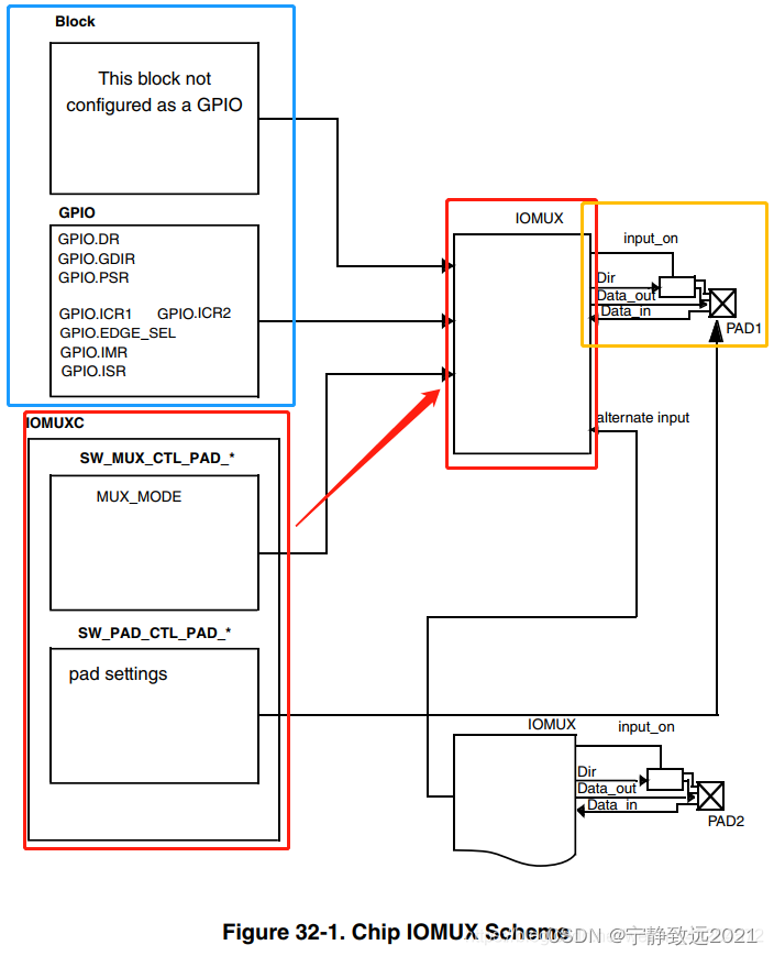
Orange part : from IOMUX control , Be responsible for controlling IO The input and output of the port enable , Pull up and down or open the drain , keep , Driving ability , Swaying rate , bandwidth ,HYS Hysteresis enable input . This part is through configuration IOMUX control .
The red part : Configure the function of the orange part , And choose this IO Who used it , adopt MUX Register selection . It also includes one that can read while outputting IO Enable end of level , If this function is enabled, the synchronous input is output
The blue part : Use this IO People who ,GPIO Box is GPIO The control end of , The output level of the control pin , Or read the level of the pin .Bolck The end is reused for other peripherals , such as PWM,SPI, And other peripherals .
To sum up, it is , The blue part uses the orange part through the configured red part IO.
How to use a pin as GPIO?:
Now configure it as normal IO Use . Learn common IO After the framework of , If you want to use it for other functions , Directly through MXC Configure and reuse to the corresponding peripheral , then , It's entirely up to the peripherals to manage .
Configuration steps
1. open GPIO1 The clock : By configuring CCM->CCGR1[27:26] open GPIO1 The clock of
2. To configure IOMUX-MUX register : Select the reuse function and whether to use SION
3. To configure IOMUX-PAD register : To configure PAD Module function
4. To configure GPIO->GDIR register : Set up GPIO Whether the controller is output control logic or input control logic
Code display .
/*  Turn on GPIO1 Port clock  */
CCM_CCGR1 &= ~(unsigned int)(3<<26);
CCM_CCGR1|=(unsigned int)(1<<26);

/*  Set up MUX The register is 0x05, Indicates that the pin is used for common GPIO */
IOMUXC_MUX_GPIO_AD_B0_09=(unsigned int)0x05;

/*  Set up PAD Properties of the register control pin   Property configuration description :  Hexadecimal number 0x000B0= Binary number 0000 0000 0000 1011 0000 b bit0:SRE:0b Swaying rate :  Slow slew rate  bit1~bit2:-:00b Register reservation  bit3~bit5:DSE:110b Driving strength :R0/6( Valid only as output ) bit6~bit7:SPEED:10b bandwidth :medium(100MHz) bit8~bit10:-:000 b Register reservation  bit11:ODE:0 b Open drain configuration : close  ( Open drain high resistance state is often used in bus configuration , Such as I2C) bit12:PKE:0b PULL / Holder configuration : close  bit13:PUE:0b PULL / Holder selection : The pull-up and pull-down and retainer are closed , Any value is invalid  bit14~bit15:PUS:00b PULL / Drop down to select : The pull-up and pull-down and retainer are closed , Any value is invalid  bit16:HYS:0b Hysteretic configuration : close  ( Valid only when entered , Schmidt trigger , When enabled, input noise can be filtered ) bit17~bit31:-:0b Register reservation  */
IOMUXC_PAD_GPIO_AD_B0_09=(unsigned int)0x000B0;

/* Set up GPIO1_09 The direction of the pin , Use output mode  */
GPIO1_GDIR|=(unsigned int)(1<<9);

/* The control pin is low , Lighten up LED The lamp */
GPIO1_DR&=~(unsigned int)(1<<9);
Use
Output : Set up GPIO->DR Set the corresponding bit of IO The level of
Input : Read GPIO-DR perhaps GPIO->PSR Register gets the corresponding IO The level of
Library function operation
1、 initialization MUX
IOMUXC_SetPinMux(IOMUXC_GPIO_AD_B0_09_GPIO1_IO09, 0U);
Here is an episode about i.MX The pin naming method of series chips .
i.MX Each pin of , They all have a special name , such as GPIO_AD_B0_09.
Input and output pins of each peripheral , There is also a special name , such as ADC2_IN0,GPIO1_IO00.
They go through a IOMUX Controller to connect , Each external pin can select a multiplexing mode to connect the required peripherals .
When a pin is connected to a certain peripheral , You can use a name to determine which pin this pin is , What's the function .
therefore , The library function configures the multiplexing of one pin through a macro
IOMUXC_GPIO_AD_B0_09_GPIO1_IO09
among :
IOMUXC representative IOMUXC controller
GPIO_AD_B0_09 Represents the pin name
GPIO1_IO09 Represents the multiplexing function of pin setting .
The library function is done in one sentence mux Configuration of , There is still left PAD The configuration of one pin is completed .
2、 initialization PAD
Actually ,PAD The configuration of is also a sentence . Go straight to the code : Configure one pin as UART1_TX.
/*  This is SDK Cut out the example of  */
IOMUXC_SetPinConfig(
      IOMUXC_GPIO_AD_B0_12_LPUART1_TX, /* GPIO_AD_B0_12 PAD functional properties : */
      0x10B0u); /* Slew Rate Field: Slow Slew Rate Drive Strength Field: R0/6 Speed Field: medium(100MHz) Open Drain Enable Field: Open Drain Disabled Pull / Keep Enable Field: Pull/Keeper Enabled Pull / Keep Select Field: Keeper Pull Up / Down Config. Field: 100K Ohm Pull Down Hyst. Enable Field: Hysteresis Disabled */
The first macro is to match MUX The macro is the same as , It's easy to understand , It can be determined according to what function the pin is multiplexed into . The key is the second parameter , This is basically operating registers !!! This value is written directly to the corresponding pin PAD register , Yes, it's written directly . Here's a recommended one i.MX Pins Tool v4.0 Tools , You can graphically pair i.MX Series of chips IO Port configuration , Output C Format code or device tree configuration file .

3、 initialization GPIO peripherals
be familiar with ST People in the standard library must be very comfortable to see this paragraph . This completes the configuration GPIO Peripherals .
//API
/*! @brief GPIO Init structure definition. */
typedef struct _gpio_pin_config
{

    gpio_pin_direction_t direction; /*!< Specifies the pin direction. */
    uint8_t outputLogic;            /*!< Set a default output logic, which has no use in input */
    gpio_interrupt_mode_t
    interruptMode;								  /*!< Specifies the pin interrupt mode, a value of @ref gpio_interrupt_mode_t. */
} gpio_pin_config_t;
void GPIO_PinInit(GPIO_Type *base, uint32_t pin, const gpio_pin_config_t *Config);
// Use
{

  /*  Definition gpio Initialize configuration structure  */
  gpio_pin_config_t led_config;

   /**  Core board LED The lamp ,GPIO To configure  **/
  led_config.direction = kGPIO_DigitalOutput; // The output mode
  led_config.outputLogic =  1;                // Default high level
  led_config.interruptMode = kGPIO_NoIntmode; // Do not use interrupt

  /*  initialization  LED GPIO. */
  GPIO_PinInit(GPIO1, 9, &led_config);
}
4、 Configure clock
4.1、 Configure the peripheral clock
/*  from AHB_CLK_ROOT in 4 Divide the frequency to get IPG_CLK_ROOT The clock , Provided to most of the internal peripherals  */
CLOCK_SetDiv(kCLOCK_IpgDiv, 3);
4.2、 Can make GPIO The clock
This clock is automatically configured in the library function , If no macro is defined FSL_SDK_DISABLE_DRIVER_CLOCK_CONTROL, Or a macro is defined, but the macro FSL_SDK_DISABLE_DRIVER_CLOCK_CONTROL It's not equal to 0, Through GPIO_PinInit Function automatically configures the corresponding function GPIO The clock .
void GPIO_PinInit(GPIO_Type *base, uint32_t pin, const gpio_pin_config_t *Config)
{

#if !(defined(FSL_SDK_DISABLE_DRIVER_CLOCK_CONTROL) && FSL_SDK_DISABLE_DRIVER_CLOCK_CONTROL)
    /* Enable GPIO clock. */
    CLOCK_EnableClock(s_gpioClock[GPIO_GetInstance(base)]);
#endif /* FSL_SDK_DISABLE_DRIVER_CLOCK_CONTROL */
···
}
5、 operation GPIO Pin status
GPIO_PinWrite(GPIO1, 9, 0U);
3、 ... and 、 drive 74hc595, Cascade mode
1. Driver header file 74hct595.h
/* * Copyright 2017-2018 NXP * All rights reserved. * * SPDX-License-Identifier: BSD-3-Clause */

#ifndef _74HCT595_H_
#define _74HCT595_H_

#include "clock_config.h"
#include "fsl_common.h"
#include "fsl_gpio.h"
#include "fsl_clock.h"
#include "fsl_iomuxc.h"
#include "pin_mux.h"


/******************************************************************************* * Definitions ******************************************************************************/
#define BOARD_595_OE_GPIO_PIN (25U)
#define BOARD_595_OE_GPIO GPIO1
#define BOARD_595_OE_PIN_MUX IOMUXC_GPIO_AD_B1_09_GPIO1_IO25

#define BOARD_595_MR_GPIO_PIN (31U)
#define BOARD_595_MR_GPIO GPIO1
#define BOARD_595_MR_PIN_MUX IOMUXC_GPIO_AD_B1_15_GPIO1_IO31

#define BOARD_595_SH_CP_GPIO_PIN (30U)
#define BOARD_595_SH_CP_GPIO GPIO1
#define BOARD_595_SH_CP_PIN_MUX IOMUXC_GPIO_AD_B1_14_GPIO1_IO30


#define BOARD_595_STCP_GPIO_PIN (29U)
#define BOARD_595_STCP_GPIO GPIO1
#define BOARD_595_STCP_PIN_MUX IOMUXC_GPIO_AD_B1_13_GPIO1_IO29


#define BOARD_595_SDI_GPIO_PIN (28U)
#define BOARD_595_SDI_GPIO GPIO1
#define BOARD_595_SDI_PIN_MUX IOMUXC_GPIO_AD_B1_12_GPIO1_IO28

#define LED_RUN_GPIO_PIN (9U)
#define LED_RUN_GPIO GPIO1
#define LED_RUN_PIN_MUX IOMUXC_GPIO_AD_B0_09_GPIO1_IO09
#define LED_RUN_ON GPIO_PinWrite(LED_RUN_GPIO, LED_RUN_GPIO_PIN, 1U)
#define LED_RUN_OFF GPIO_PinWrite(LED_RUN_GPIO, LED_RUN_GPIO_PIN, 0U)


#define LED_ALARM_GPIO_PIN (10U)
#define LED_ALARM_GPIO GPIO1
#define LED_ALARM_PIN_MUX IOMUXC_GPIO_AD_B0_10_GPIO1_IO10
#define LED_ALARM_ON GPIO_PinWrite(LED_ALARM_GPIO, LED_ALARM_GPIO_PIN, 1U)
#define LED_ALARM_OFF GPIO_PinWrite(LED_ALARM_GPIO, LED_ALARM_GPIO_PIN, 0U)


#define LED_COMM_GPIO_PIN (11U)
#define LED_COMM_GPIO GPIO1
#define LED_COMM_PIN_MUX IOMUXC_GPIO_AD_B0_11_GPIO1_IO11
#define LED_COMM_ON GPIO_PinWrite(LED_COMM_GPIO, LED_COMM_GPIO_PIN, 1U)
#define LED_COMM_OFF GPIO_PinWrite(LED_COMM_GPIO, LED_COMM_GPIO_PIN, 0U)

extern void hct595_Init(void);
extern void hct595_SetValue(uint16_t value);
extern void delay(uint32_t count);

#endif /* _74HCT595_H_ */
2. Drive source file 74hct595.c
/* * Copyright 2017-2018 NXP * All rights reserved. * * SPDX-License-Identifier: BSD-3-Clause */

#include "74hct595.h"

void hct595_Init(void);
static void GPIO_Mode_Config(void);


void hct595_SetValue(uint16_t value)
{


	for(int i = 0; i < 16; i++)
		{

		GPIO_PinWrite(BOARD_595_SH_CP_GPIO, BOARD_595_SH_CP_GPIO_PIN, 0U);  //SH=0
		if(value & 0x8000)
			GPIO_PinWrite(BOARD_595_SDI_GPIO, BOARD_595_SDI_GPIO_PIN, 1U);
		else
			GPIO_PinWrite(BOARD_595_SDI_GPIO, BOARD_595_SDI_GPIO_PIN, 0U);

		delay(700000);
		GPIO_PinWrite(BOARD_595_SH_CP_GPIO, BOARD_595_SH_CP_GPIO_PIN, 1U);  //SH=1
		delay(700000);
		value = value << 1;
		}
		GPIO_PinWrite(BOARD_595_STCP_GPIO, BOARD_595_STCP_GPIO_PIN, 0U);  //ST=0
	delay(700000);
	GPIO_PinWrite(BOARD_595_STCP_GPIO, BOARD_595_STCP_GPIO_PIN, 1U);  //ST=1
	delay(700000);

}


void hct595_Init(void)
{

IOMUXC_SetPinMux(BOARD_595_OE_PIN_MUX, 0U);
IOMUXC_SetPinConfig(BOARD_595_OE_PIN_MUX, 0x10B0u);
IOMUXC_SetPinMux(BOARD_595_MR_PIN_MUX, 0U);
IOMUXC_SetPinConfig(BOARD_595_MR_PIN_MUX, 0x10B0u);
IOMUXC_SetPinMux(BOARD_595_SH_CP_PIN_MUX, 0U);
IOMUXC_SetPinConfig(BOARD_595_SH_CP_PIN_MUX, 0x10B0u);
IOMUXC_SetPinMux(BOARD_595_STCP_PIN_MUX, 0U);
IOMUXC_SetPinConfig(BOARD_595_STCP_PIN_MUX, 0x10B0u);
IOMUXC_SetPinMux(BOARD_595_SDI_PIN_MUX, 0U);
IOMUXC_SetPinConfig(BOARD_595_SDI_PIN_MUX, 0x10B0u);
//led
IOMUXC_SetPinMux(LED_RUN_PIN_MUX, 0U);
IOMUXC_SetPinConfig(LED_RUN_PIN_MUX, 0x10B0u);
IOMUXC_SetPinMux(LED_ALARM_PIN_MUX, 0U);
IOMUXC_SetPinConfig(LED_ALARM_PIN_MUX, 0x10B0u);
IOMUXC_SetPinMux(LED_COMM_PIN_MUX, 0U);
IOMUXC_SetPinConfig(LED_COMM_PIN_MUX, 0x10B0u);
//GPIO Input / output attribute configuration
GPIO_Mode_Config();

//MR = 1
GPIO_PinWrite(BOARD_595_MR_GPIO, BOARD_595_MR_GPIO_PIN, 0U);
delay(700000);
GPIO_PinWrite(BOARD_595_MR_GPIO, BOARD_595_MR_GPIO_PIN, 1U);
GPIO_PinWrite(BOARD_595_OE_GPIO, BOARD_595_OE_GPIO_PIN, 0U);

}

static void GPIO_Mode_Config(void)
{

  /*  Definition gpio Initialize configuration structure  */
  gpio_pin_config_t led_config;

   /**  Core board LED The lamp ,GPIO To configure  **/
  led_config.direction = kGPIO_DigitalOutput; // The output mode
  led_config.outputLogic =  1;                // Default high level
  led_config.interruptMode = kGPIO_NoIntmode; // Do not use interrupt

  /*  initialization  LED GPIO. */
  GPIO_PinInit(LED_RUN_GPIO, LED_RUN_GPIO_PIN, &led_config);
  GPIO_PinInit(LED_ALARM_GPIO, LED_ALARM_GPIO_PIN, &led_config);
  GPIO_PinInit(LED_COMM_GPIO, LED_COMM_GPIO_PIN, &led_config);

  GPIO_PinInit(BOARD_595_OE_GPIO, BOARD_595_OE_GPIO_PIN, &led_config);
  GPIO_PinInit(BOARD_595_MR_GPIO, BOARD_595_MR_GPIO_PIN, &led_config);
  GPIO_PinInit(BOARD_595_SDI_GPIO, BOARD_595_SDI_GPIO_PIN, &led_config);
  GPIO_PinInit(BOARD_595_SH_CP_GPIO, BOARD_595_SH_CP_GPIO_PIN, &led_config);
  GPIO_PinInit(BOARD_595_STCP_GPIO, BOARD_595_STCP_GPIO_PIN, &led_config);

}
版权声明
本文为[Quiet Zhiyuan 2021]所创,转载请带上原文链接,感谢
https://yzsam.com/2022/04/202204232019571541.html
边栏推荐
- 2022 - Data Warehouse - [time dimension table] - year, week and holiday
- Numpy mathematical function & logical function
- Identification of bolt points in aerial photography based on perception
- Matlab analytic hierarchy process to quickly calculate the weight
- Customize timeline component styles
- Browser - learning notes
- Redis的安装(CentOS7命令行安装)
- 考研英语唐叔的语法课笔记
- DNS cloud school | quickly locate DNS resolution exceptions and keep these four DNS status codes in mind
- Error reported by Azkaban: Azkaban jobExecutor. utils. process. ProcessFailureException: Process exited with code 64
猜你喜欢
Identification of bolt points in aerial photography based on perception
Don't bother tensorflow learning notes (10-12) -- Constructing a simple neural network and its visualization
Handwritten Google's first generation distributed computing framework MapReduce
![[graph theory brush question-5] Li Kou 1971 Find out if there is a path in the graph](/img/fb/9822cccde4ca39d8066024c09a7349.png)
[graph theory brush question-5] Li Kou 1971 Find out if there is a path in the graph
DNS cloud school rising posture! Three advanced uses of authoritative DNS

PIP installation package reports an error. Could not find a version that satisfies the requirement pymysql (from versions: none)
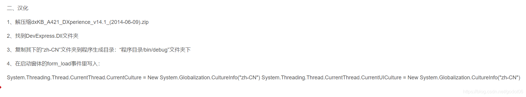
Devexpress 14.1 installation record
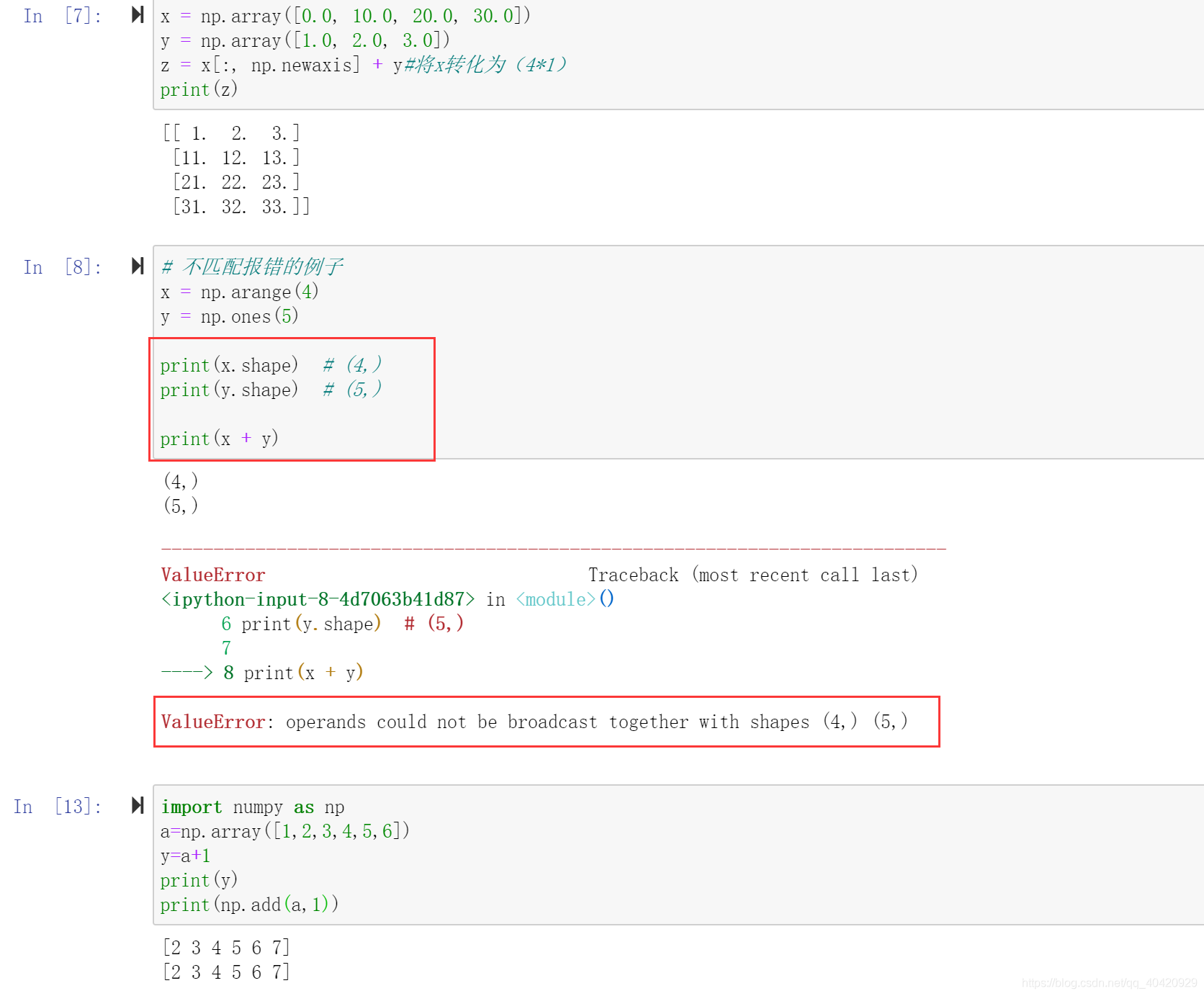
Numpy mathematical function & logical function
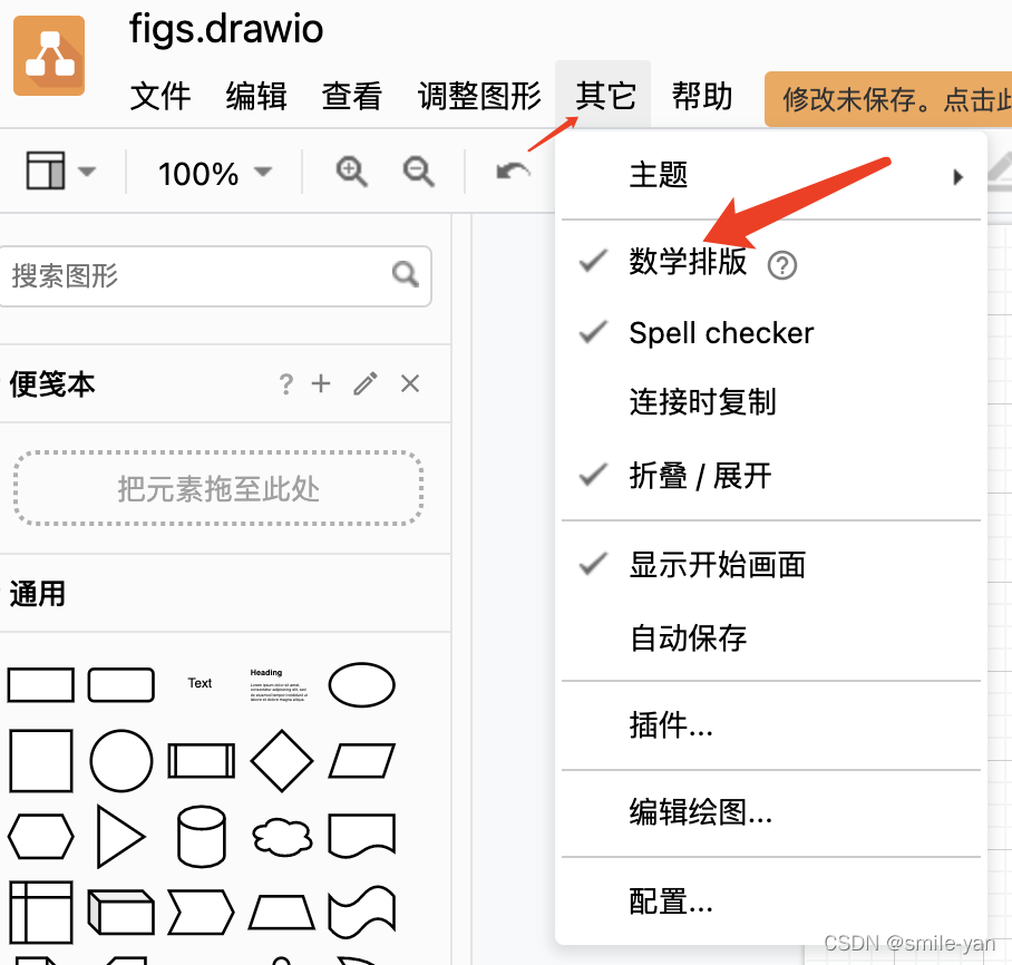
Recommend an open source free drawing software draw IO exportable vector graph
LeetCode动态规划训练营(1~5天)
随机推荐
SIGIR'22 "Microsoft" CTR estimation: using context information to promote feature representation learning
[problem solving] 'ASCII' codec can't encode characters in position XX XX: ordinal not in range (128)
Scrapy教程 - (2)寫一個簡單爬蟲
Redis installation (centos7 command line installation)
DTMF双音多频信号仿真演示系统
微信中金财富高端专区安全吗,证券如何开户呢
go-zero框架数据库方面避坑指南
ABAQUS script email auto notification
三十一. `prototype`显示原型属性和`__proto__`隐式原型属性
Livego + ffmpeg + RTMP + flvjs to realize live video
Cadence OrCAD capture batch change component packaging function introduction graphic tutorial and video demonstration
Building the tide, building the foundation and winning the future -- the successful holding of zdns Partner Conference
16MySQL之DCL 中 COMMIT和ROllBACK
The second method of file upload in form form is implemented by fileitem class, servletfileupload class and diskfileitemfactory class.
R language ggplot2 visualization: ggplot2 visualizes the scatter diagram and uses geom_ mark_ The ellipse function adds ellipses around data points of data clusters or data groups for annotation
还在用 ListView?使用 AnimatedList 让列表元素动起来
DTMF dual tone multi frequency signal simulation demonstration system
Analysis of the relationship between generalized Bim and CAD under the current background
Operation of numpy array
redis 分布式锁