当前位置:网站首页>Quartus prime hardware experimental development (de2-115 board) experiment 1 CPU instruction calculator design
Quartus prime hardware experimental development (de2-115 board) experiment 1 CPU instruction calculator design
2022-04-23 13:56:00 【Slag Ye】
Experiment 1 CPU Instruction arithmetic unit design
- The experiment purpose
- master QuartusII And other experimental tools 、 comprehensive 、 Simulation 、 How to use the download
- master DE2 The functional characteristics and application methods of the developed version of the device
- master Verilog HDL The main methods and techniques of combinational logic system design
- Master and apply the design method and process
- Preview requirements
- understand QuartusII Equal Discipline Distribution 、 Download method and process
- Understand the input of development board 、 The output shows the working characteristics of the resource
- Understand development board design 、 Development and testing methods and processes
- The experimental requirements
Design a simple CPU Instruction arithmetic unit , The command format is as follows .
Operation type 1
Operands 1
Operation type 2
Operands 3
Operands 4
The specific functions completed are defined as follows :
- Operation type 1: The operands 1 As an unsigned binary number , In the seven segment tube, the binary sequence equivalent value is displayed in decimal system .
- Operation type 2: Implement operands 3、 Operands 4 Add between 、 reduce 、 Multiply operation , In the seven section pipe with ten / Hexadecimal Displays operands and results . Operands 3 and 4 by BCD Code means 2 A decimal number ( The value is 00-99).
Be careful :
- Operation type 2 in , Negative numbers in subtraction logic , Is displayed “-”, Positive numbers can not display symbols
- Operation type 2 in , Add 、 reduce 、 Multiplication operands and results are displayed in decimal , It can be realized by cyclic display on the seven section tube .
- Note the operands 3、4 With BCD Code input , exceed 9 Of BCD Code output processing problem .
- Try the addition operation, which is realized by pipeline . Pay attention to the number of significant digits .
- If you feel that the display ability of seven segment tube is weak , You can query LCD1602 Control module code , use LCD Show .
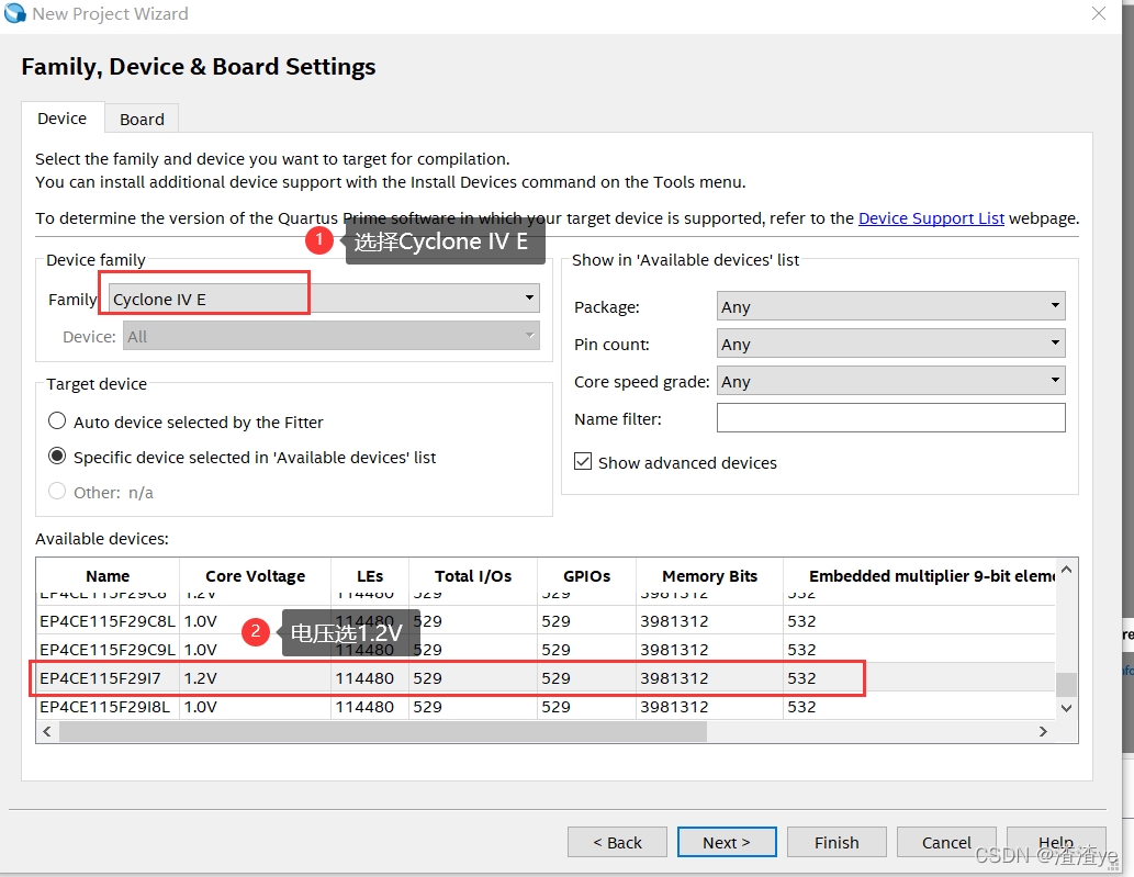
1. First plug the board into the computer ( Black line power supply , White line computer )

2. In the start setting board , choice Cyclone IV E, Then select the voltage below 1.2V The can
3. After completing the configuration of the board , Enter the main file code :
module zhiling(key,x2,x3,Hex0,Hex1,Hex2,Hex3,Hex4,Hex5,Hex6,Hex7,x);
input [7:0] x2,x3;
input key;
reg[7:0] x1;
input [1:0] x;// Indicates the display mode of the seven section tube
output reg[6:0] Hex0,Hex1,Hex2,Hex3,Hex4,Hex5,Hex6,Hex7;
reg[11:0] add;
reg[7:0] sub;
reg[13:0] mul;
wire[7:0] n3,n2;
integer flag;// Symbol sign bit
// Additive variable
reg cout1,cout2;
reg [6:0] fh;
reg [3:0] low,low0,mid,mid0;
reg [3:0] a1,a2,a3,a4;// Multiplication, you express
reg [3:0] t1,t2,t3;//x1 Value
reg [3:0] s1,s2;
assign n2=x2[7:4]*10+x2[3:0];
assign n3=x3[7:4]*10+x3[3:0];
always@(*)
begin
   if(key==1)
	begin
   x1=x2;
   t1=x1%4'b1010;
	t2=x1/4'b1010%4'b1010;
	t3=x1/4'b1010/4'b1010;
	end
end
// Add , Two stage pipeline mode
always@(*)
begin
{cout1,low0}=x2[3:0]+x3[3:0];
if(cout1==1) begin low=low0+4'b0110; end
else if(low0>9&&cout1==0) begin {cout1,low}=low0+4'b0110;end
else begin low=low0;cout1=0;end
end

always@(*)
begin
{cout2,mid0}=x2[7:4]+x3[7:4]+cout1;
if(cout2==1) begin mid=mid0+4'b0110; end
else if(mid0>9&&cout2==0) begin {cout2,mid}=mid0+4'b0110;end
else begin mid=mid0;cout2=0;end
add={cout2,mid,low};
end
// Subtraction
always@(*)
begin
flag=0;
if(n2>=n3) sub=n2-n3;
else begin flag=1;sub=n3-n2;end
fh=(flag==1)?7'b0111111:7'b1111111;
   s1=sub%4'b1010;
	s2=sub/4'b1010;
end
// Multiplication
always@(*)
begin
   mul=n2*n3;
   a1=mul%4'b1010;
	a2=mul/4'b1010%4'b1010;
	a3=mul/4'b1010/4'b1010%4'b1010;
	a4=mul/4'b1010/4'b1010/4'b1010;
end

always@(x)
begin
case(x)
2'b00:begin {Hex2,Hex1,Hex0}={show(t3),show(t2),show(t1)};Hex3=7'b1111111;Hex4=7'b1111111;Hex5=7'b1111111;Hex6=7'b1111111;Hex7=7'b1111111;end
2'b01:begin {Hex7,Hex6}={show(x2[7:4]),show(x2[3:0])};{Hex5,Hex4}={show(x3[7:4]),show(x3[3:0])};
				{Hex2,Hex1,Hex0}={show(add[11:8]),show(add[7:4]),show(add[3:0])};Hex3=7'b1111111;  end
2'b10:begin {Hex7,Hex6}={show(x2[7:4]),show(x2[3:0])};{Hex5,Hex4}={show(x3[7:4]),show(x3[3:0])};
				{Hex2,Hex1,Hex0}={fh,show(s2),show(s1)};Hex3=7'b1111111;  end
2'b11:begin {Hex7,Hex6}={show(x2[7:4]),show(x2[3:0])};{Hex5,Hex4}={show(x3[7:4]),show(x3[3:0])};
				{Hex3,Hex2,Hex1,Hex0}={show(a4),show(a3),show(a2),show(a1)};  end
endcase
end

function [6:0]show;
   input[3:0] a0;
	reg[6:0] b;
	begin
	case(a0)
  4'd0:b=7'b1000000;
  4'd1:b=7'b1111001;
  4'd2:b=7'b0100100;
  4'd3:b=7'b0110000;
  4'd4:b=7'b0011001;
  4'd5:b=7'b0010010;
  4'd6:b=7'b0000010;
  4'd7:b=7'b1111000;
  4'd8:b=7'b0000000;
  4'd9:b=7'b0011000;
default:b=7'b1111111;
	endcase
	show=b;
	end
	endfunction
endmodule
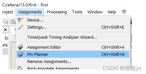
4. Click on import assignment

5. Import pin assignment , Data set download link of Experiment 1 :

6. Then open Pin Planner, Check whether the pins are connected normally
7.first The interface defined by the module corresponds to the pin allocation file . After importing the pin assignment file , see pin planner Connection of middle pin . If a blank line appears , Description pin file error , Need modification , Re import .( It has been tested , If you use the above link to import pins , Normal operation , This step can be omitted )
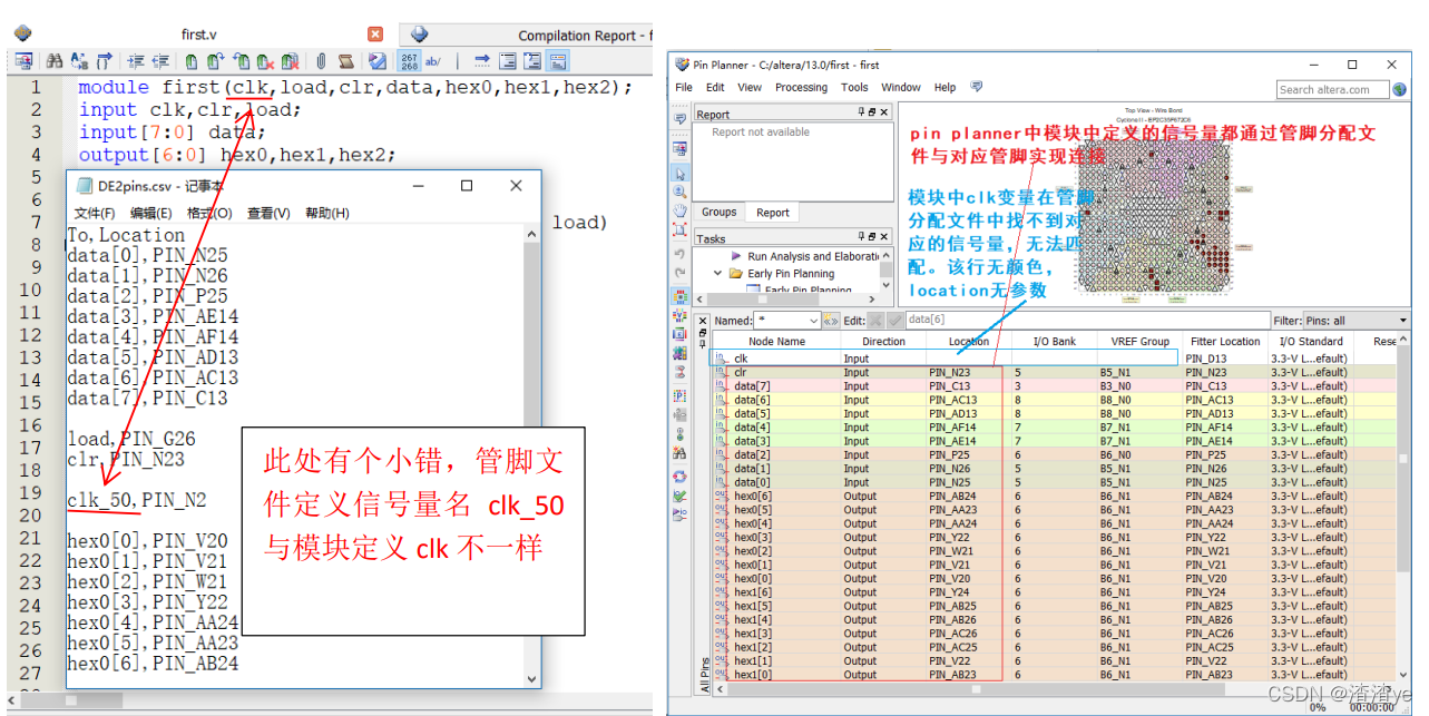
8. If the pin assignment file is modified , You need to remove the imported pin file ,remove assignments. Reopen pin planer You will find that the connection is clear , All lines become colorless .( It has been tested , If you use the above link to import pins , Normal operation , This step can be omitted )


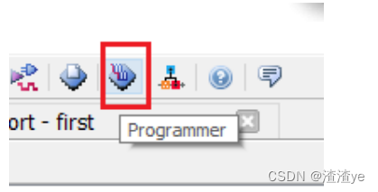
9. Import the pin assignment table correctly , After no mistakes . Re integrate the whole project

10. Integrated , After no mistakes . Connect the development board , Turn on the power , Ready to download .
stay programmer window , Maybe as shown in the box no hardware, No hardware . Click on hardware setup function . eject hardware setup window , Add hardware .

11. If there is no USB drive , Manual operation is required Update driver
Right click “ My computer ” Icon , choice “ management ”


12. choice “ Manual search ”, Get into Quartus prime Install catalog file , find “USB”

13. Two “USB” Just choose one ( Then in the hardware 115 Just choose one from the socket of the board )

14. After installation , that will do

15. After completing the driver update , Click again on the Programmer window , Click on hardware setup function . eject hardware setup window , Add hardware


16. Click... To finish the configuration Start that will do

Then start the hardware test , Experiment one is CPU Instruction arithmetic unit , The operation of addition, subtraction and multiplication
Multiplication :
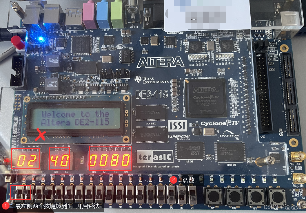
Add :

Subtraction :

版权声明
本文为[Slag Ye]所创,转载请带上原文链接,感谢
https://yzsam.com/2022/04/202204231353463466.html
边栏推荐
- [code analysis (7)] communication efficient learning of deep networks from decentralized data
- YARN线上动态资源调优
- 【项目】小帽外卖(八)
- Oracle database recovery data
- The difference between is and as in Oracle stored procedure
- AttributeError: ‘dict‘ object has no attribute ‘iteritems‘
- Generate 32-bit UUID in Oracle
- Crontab timing task output generates a large number of mail and runs out of file system inode problem processing
- Express②(路由)
- 淘宝发布宝贝提示“您的消保保证金额度不足,已启动到期保障”
猜你喜欢

2021年秋招,薪资排行NO
![MySQL index [data structure + index creation principle]](/img/11/6bdc8a62e977ffb67be07ded0c8978.png)
MySQL index [data structure + index creation principle]

Handling of high usage of Oracle undo
Android interview theme collection
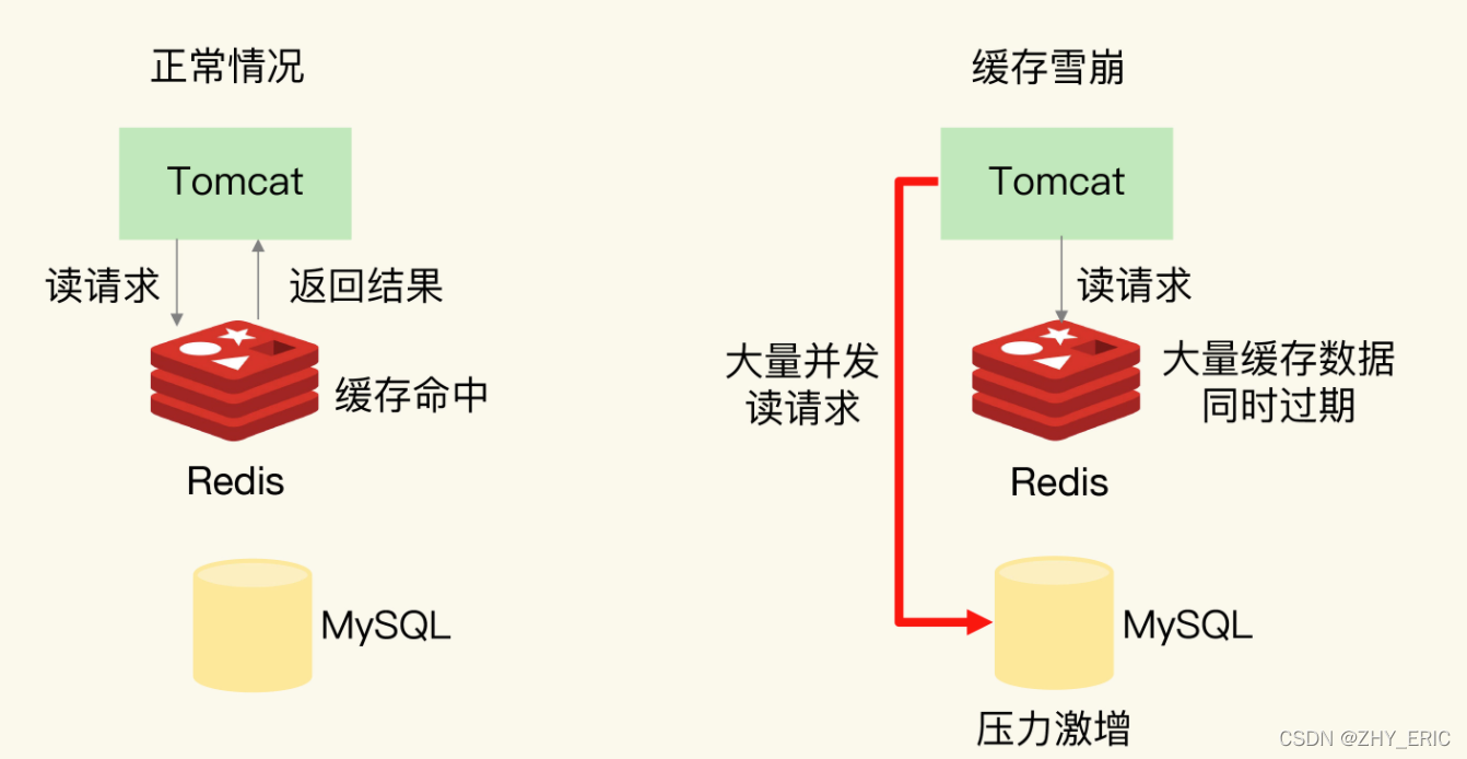
redis如何解决缓存雪崩、缓存击穿和缓存穿透问题
![MySQL [read / write lock + table lock + row lock + mvcc]](/img/a9/ace85899a01a7d4fd80b2e631e44d6.png)
MySQL [read / write lock + table lock + row lock + mvcc]
Wechat applet

JUC interview questions about synchronized, ThreadLocal, thread pool and atomic atomic classes
Choreographer全解析

freeCodeCamp----time_ Calculator exercise
随机推荐
Es introduction learning notes
freeCodeCamp----arithmetic_ Arranger exercise
leetcode--357. 统计各位数字都不同的数字个数
[code analysis (2)] communication efficient learning of deep networks from decentralized data
PG SQL intercepts the string to the specified character position
[code analysis (6)] communication efficient learning of deep networks from decentralized data
【项目】小帽外卖(八)
Jenkins construction and use
Generate 32-bit UUID in Oracle
UML统一建模语言
JS 力扣刷题 102. 二叉树的层序遍历
ACFs file system creation, expansion, reduction and other configuration steps
Dolphin scheduler integrates Flink task pit records
SSM project deployed in Alibaba cloud
第一章 电商秒杀商品回顾
The art of automation
freeCodeCamp----time_ Calculator exercise
村上春树 --《当我谈跑步时,我谈些什么》句子摘录
Reading notes: Secure federated matrix factorization
Oracle modify default temporary tablespace