当前位置:网站首页>The FPGA - work summary recently
The FPGA - work summary recently
2022-08-09 13:44:00 【51CTO】
工作概述:
1)看《电子技术基础》和《fpga数字逻辑设计》Learn the combinatorial logic portion of digital circuits,Simplification and dimensionality reduction of Karnaugh maps.
2)Review the adder,全加器,译码器,编码器,数据选择器,数值比较器,Consolidate how these combinatorial logics work and are usefulverilog在ISE的实现.
3)看《verilog基本语法》学习和巩固verilog的基本语法.
1.摘抄:
The output of a combinational circuit at a certain moment is only related to the input at that moment,It has nothing to do with the state of the circuit at the previous moment.
Characteristics of combinational circuits
1) 电路由逻辑门构成,不含记忆元件
2) There is no feedback delay loop between output and input
3) The output is independent of the original state of the circuit

When the two inputs of a logic gate change in opposite directions at the same time,The time of change varies.This phenomenon is called competition.The phenomenon of output disturbance pulses due to competition is called risk.
-《电子技术基础》and digitalppt
1.理解:
数字电路根据逻辑功能的不同特点,可以分成两大类,一类叫组合逻辑电路(简称组合电路),另一类叫做时序逻辑电路(简称时序电路).
组合逻辑电路在逻辑功能上的特点是任意时刻的输出仅仅取决于该时刻的输入,与电路原来的状态无关.
时序逻辑电路在逻辑功能上的特点是任意时刻的输出不仅取决于当时的输入信号,而且还取决于电路原来的状态,或者说,还与以前的输入有关.
The basic idea of logic circuit design:
1)Analyse the actual function of the actual problem
2)Write the truth table according to actual needs
3)Write logical expressions from truth tables
4)Avoid competing risks by simplifying expressions according to Karnaugh maps
2.摘抄:
How to understand the adventure and competition mentioned here?
First, let's talk about the reasons for taking risks and competition:when we are in digital logic circuits,We think that the input and output of the circuit are all smooth logic levels,But the signal is actually being delivered,It takes a certain amount of time to pass through the logic circuit.Or because of the difference in the delay of the gate,There will be states that differ from the steady state situation,produces an output error,It's called competitive adventure in the circuit.
--《电子技术基础》
2.理解:
Risking doesn't necessarily have an effect on the actual output logic,However, in order to avoid the risk of competition, the input and output in the actual circuit are affected,This should be avoided as much as possible.in logical design,在PCWhen the terminal is simulated, its role cannot be reflected,But in actual work operation,This cannot be ignored.
So to sum up the ways to eliminate competitive risk:
1)Find and eliminate complementary multiplication terms.
2)增加乘积项避免互补项相加.
3)A capacitor is connected in parallel at the output.
3.摘抄:
It is because of the logical functional characteristics of combinational logic and sequential logic that combinational logic circuits use blocking assignment,时序逻辑电路使用非阻塞赋值.
What is blocking assignment and non-blocking assignment
阻塞赋值操作符用等号(即 = )表示.“阻塞”是指在进程语句(initial和always)中,当前的赋值语句阻断了其后的语句,也就是说后面的语句必须等到当前的赋值语句执行完毕才能执行.
非阻塞赋值操作符用小于等于号 (即 <= )表示.“非阻塞”是指在进程语句(initial和always)中,当前的赋值语句不会阻断其后的语句,It can be simply understood that several non-blocking assignment statements can be executed at the same time.
A non-blocking assignment operation procedure:
1)在赋值开始时刻,Evaluates the expression on the right-hand side of a nonblocking assignment.
2)在赋值结束时刻,Updates the left-hand expression of a nonblocking assignment.
-《verilog基本语法》
3.理解:
EG:如果a=3 b=8;a=b,c=a;
- If the blocking assignment is executed when the first item is executedaThe value of immediately becomes a=8;when the second rule is implementedc=8;
- If it is a non-blocking assignment method, it is based on the operation process of non-blocking assignment:The calculation starts to calculate the values on the right, respectively8 3,The second step refreshes the value of the expression on the lefta=8 c=3;
4.摘抄:
Memory型变量
尽管memory型数据和reg型数据的定义格式很相似,But be aware of the differences.MemoryDepicted is depth,regDepicted is the width.
Reg [ n-1:0 ] rega; //一个n位寄存器
Reg mema [ n-1 ] //一个由nA memory bank consisting of one-bit registers
一个nRegisters of bits can be assigned values in an assignment statement.And a full memory won't do
Rega = 0;//Legal assignment statement
Mema=0;//Illegal assignment statement
Mema[3]=0;//合法,给memoryThe third cell in is assigned the value of 0
边栏推荐
- 生成上传密钥和密钥库
- Glory to the Blue Yonder, speeds up the strategic growth
- Customize VIEW to realize in-app message reminder to rotate up and down
- Rust 入门指南(使用JSON)
- 陈强教授《机器学习及R应用》课程 第十八章作业
- Jenkins API groovy调用实践: Jenkins Core Api & Job DSL创建项目
- Flutter introduction advanced trip (5) Image Widget
- Standing wave ratio calculation method
- 使用注解将EventBus封装抽取到基类
- Flutter入门进阶之旅(四)文本输入Widget TextField
猜你喜欢
novel research
链表噩梦之一?5000多字带你弄清它的来龙去脉
5G China unicom 直放站 网管协议 实时性要求
第六届”蓝帽杯“全国大学生网络安全技能大赛 半决赛
Periodic sharing of Alibaba Da Tao system model governance
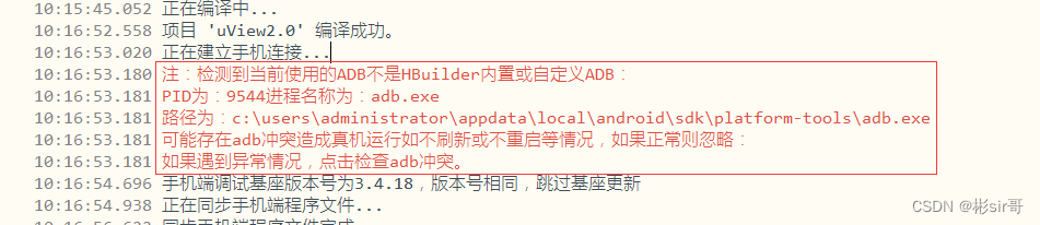
注:检测到当前使用的ADB不是HBuilder内置或自定义ADB:PID为:9544进程名称为:adb.exe 路径为:c:\users\administrator\appdata\local\and

Flutter Getting Started and Advanced Tour (8) Button Widget
jenkins api create custom pipeline
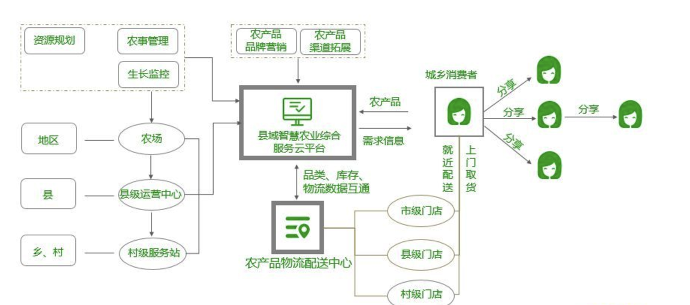
农村区县域农业电商如何做?数字化转型如何进行?

30行代码实现蚂蚁森林自动偷能量
随机推荐
About the handling of variable parameters in the Retrofit network request URL
新起之秀 DPU,正在掀起数据中心变革!
Data Mining-05
数据挖掘-06
驻波比计算方法
novel research
ftplib+ tqdm 上传下载进度条
AI basketball referee, walking is special, ask harden care don't care
合并两个有序列表
中断系统结构及中断控制详解
GIN Bind模式获取参数和表单验证
大佬们,请教一下,我看官方文档中,sqlserver cdc只支持2012版之后的,对于sqlser
二维数组&指针
生成上传密钥和密钥库
ctfshow七夕杯2022
26. Pipeline parameter substitution command xargs
glide工具类的简单封装
造自己的芯,让谷歌买单!谷歌再度开源 180nm 工艺的芯片
Go 事,如何成为一个Gopher ,并在7天找到 Go 语言相关工作,第1篇
卷积神经网络表征可视化研究综述(1)