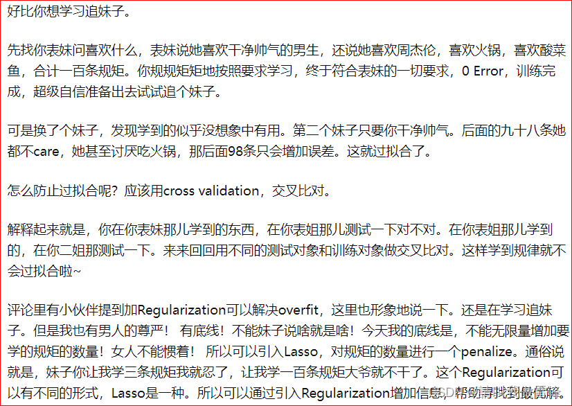
当前位置:网站首页>cadence SPB17. 4 - Active Class and Subclass
cadence SPB17. 4 - Active Class and Subclass
2022-04-23 15:34:00 【LostSpeed】
Preface
allegro When placing elements on a board , Need to be in option Specify the current class and subclasses in the page .
Want to understand the meaning of these classes and subclasses .
The official local document is file:///D:/cadence/spb_17.4/doc/algrostart/appd.html
note
The number of classes is 26
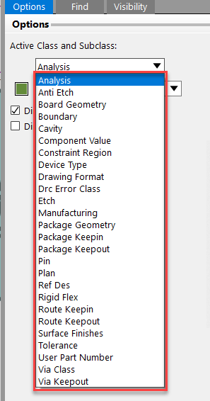
There are many subclasses under each category .
The subclass names of different classes may be the same , But the meaning is different .
class - ANALYSIS
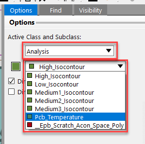
The subclasses below this class are obsolete (This subclass is no longer in use)
Subclass Analysis - _Epb_Scratch_Acon_Space_Poly The official didn't say
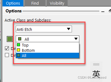
class - Anti Etch
No official documentation was found
Check information , It can be seen that this layer is matched keep in Area , Carry out network plane segmentation . You can assign a plane to a specified network (e.g. GND1, GND2), Make different signals have different large-area potential reference planes .
class - BOARD GEOMETRY
Plate and frame layer
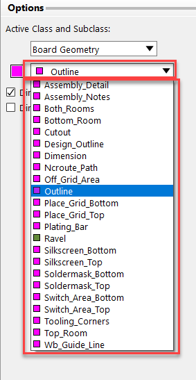
Subclass 23 individual
BOARD GEOMETRY - Assembly_Detail : Assembly layer details , Instructions for assembly requirements can be placed
BOARD GEOMETRY - Assembly_Notes : Remarks of assembly layer , Put the text description of the assembly requirements , and Assembly_Detail Almost work .
BOARD GEOMETRY - Both_Rooms : Place one... On all layers of the assembly layer room, Used to specify which devices can be placed in these room in , coordination “Package to Room” Use
BOARD GEOMETRY - Bottom_Room : and Both_Rooms similar , The difference is in the assembly layer bottom Layering room.
BOARD GEOMETRY - Cutout : The official didn't say , Look up the data , It is used for opening windows in the plate and frame layer .
BOARD GEOMETRY - Design_Outline, The official didn't say , It should be that the official documents didn't keep up with S026 Patch . This floor is used for placing the outer frame of the board . Press F2 when , Zoom directly to Design_Outline Draw the size of the shape of the closed board and frame view.
BOARD GEOMETRY - Dimension : Definition of dimension of placing frame layer .
BOARD GEOMETRY - Ncroute_Path: The official didn't say . Is it not officially stated , It means it doesn't matter ?
BOARD GEOMETRY - Off_Grid_Area: Definition grid Area , Whether it is a different area of the board , Grid point ( Show , Capture ) It can be different ?
BOARD GEOMETRY - Outline: Officials say this is the frame layer , But the information says that this floor is not recommended , You should use Design_Outline.
BOARD GEOMETRY - Place_Grid_Bottom: Place the bottom grid
BOARD GEOMETRY - Place_Grid_Top: Place top grid
BOARD GEOMETRY - Plating_Bar: Metallized strips ,e.g. Golden finger
BOARD GEOMETRY - Ravel : No official statement
BOARD GEOMETRY - Silkscreen_Bottom : Bottom screen
BOARD GEOMETRY - Silkscreen_Top : Top screen
BOARD GEOMETRY - Soldermask_Bottom : Bottom layer resistance welding
BOARD GEOMETRY - Soldermask_Top : Top layer resistance welding
BOARD GEOMETRY - Switch_Area_Bottom : Has been abandoned
BOARD GEOMETRY - Switch_Area_Top : Has been abandoned
BOARD GEOMETRY - Tooling_Corners : It seems to be related to flexible circuit board .
BOARD GEOMETRY - Top_Room : top floor room
BOARD GEOMETRY - Wb_Guide_Line : Definition APD+ Pad boundary in
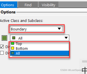
class - Boundary
No official instructions were found
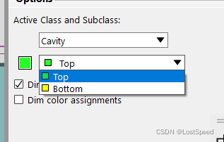
class - Cavity
No official instructions were found
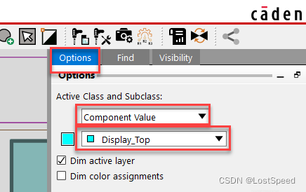
class - Component Value
This class is only used for pure manual cloth board ( Scenarios that do not use schematic diagrams ), No one does that ?
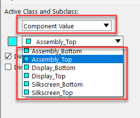
Subclass 6 individual
Component Value - Assembly_Bottom : Assemble the bottom layer , Auxiliary manual in PCB Editor Enter component values in , If it is a net list introduced from the schematic diagram , It's no use here
Component Value - Assembly_Top : Assemble the top layer , Other same as above .
Component Value - Display_Bottom : Show the underlying , Other same as above .
Component Value - Display_Top : Show top level , Other same as above .
Component Value - Silkscreen_Bottom : Silk screen bottom layer , Other same as above .
Component Value - Silkscreen_Top : Silk screen top layer , Other same as above .
class - Constraint Region
No official instructions were found
It means restricted area .
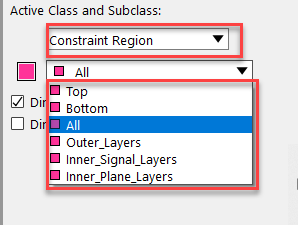
Last 3 Item means : Outer layer , Inner signal layer , Internal potential layer .
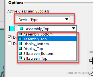
class - Device Type
This class It's in different sub-class Displays the device type in the .
class - Drawing Format
This class is used to draw drawing information . e.g. Icons for description , Title bar, etc. .
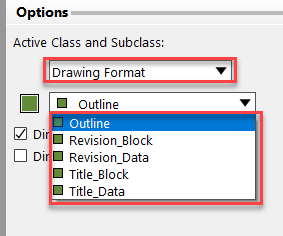
Subclass - Drawing Format:Outline Place design forms or documents
Subclass - Drawing Format:Revision_Block Differences between placement versions
Subclass - Drawing Format:Revision_Data Place version history information
Subclass - Drawing Format:Title_Block The title bar , Benchmarking schematic title block
Subclass - Drawing Format:Title_Data PCB Data in the title bar , e.g. Project name , Board name , author , date , Version number .
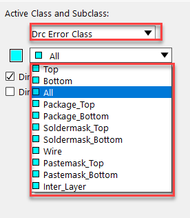
class - Drc Error Class
This layer is used to select DRC FALSE .
Subclasses know their meaning from their names
class - Etch
This class is for discharge wiring .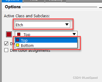
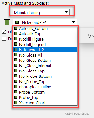
class - Manufacturing
Automatic operation ( from TCL Script operation ) The layer , Manual editing of this layer is not recommended .
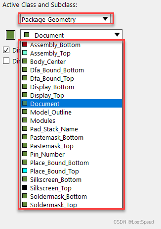
class - Package_Geometry
PCB Encapsulation layer
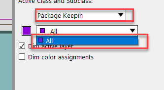
class - Package_Keepin
PCB Encapsulate the area where you can place
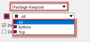
class - Package_Keepout
PCB Encapsulate areas that cannot be placed
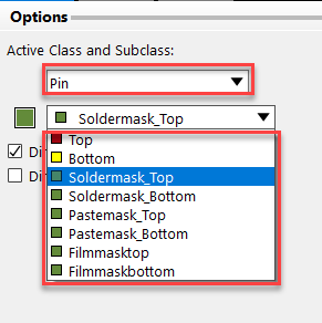
class - Pin
No official instructions were found
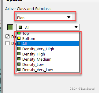
class - Plan
No official description found
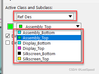
class - Ref Des
This layer is the display of component tag number .
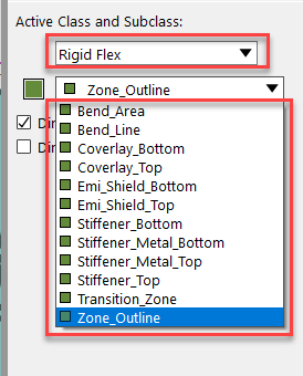
class - Rigid Flex
No official description found
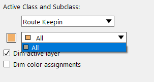
class - Route Keepin
No official description found
It literally means allow wiring area
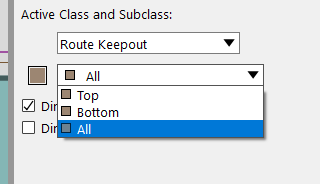
class - Route Keepout
No official description found
It literally means no wiring area
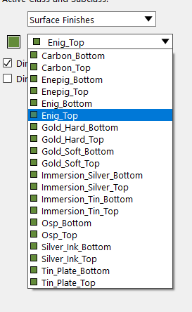
class - Surface Finishes
No official description found
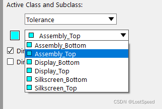
class - Tolerance
Tolerance layer
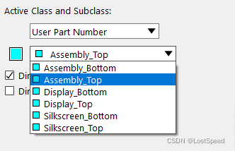
class - User Part Number
Part number layer (e.g. Jialichuang commodity No , Internal private component number )
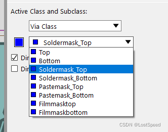
class - Via Class
No official statement
Via class
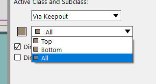
class - Via Keepout
No official statement .
It is forbidden to place vias . Do you mean , Which area can't place vias ?
END
take option On page Active Class and Subclass, Combined with official documents , I have a look at it .
I have a general idea of these various Class, SubClass Use of .
Large factory documents and software are not exactly corresponding , A lot of things are not written , Turning back and forth official documents may not necessarily find the corresponding operation or instructions .
But compared with small factory software , OK, too much .
版权声明
本文为[LostSpeed]所创,转载请带上原文链接,感谢
https://yzsam.com/2022/04/202204231526432265.html
边栏推荐
- setcontext getcontext makecontext swapcontext
- What are the mobile app software testing tools? Sharing of third-party software evaluation
- Mysql连接查询详解
- Node.js ODBC连接PostgreSQL
- Kubernetes详解(九)——资源配置清单创建Pod实战
- Mumu, go all the way
- Node. JS ODBC connection PostgreSQL
- 如果conda找不到想要安装的库怎么办PackagesNotFoundError: The following packages are not available from current
- Explanation of redis database (I)
- Llvm - generate if else and pH
猜你喜欢


随机推荐
Have you really learned the operation of sequence table?
Adobe Illustrator menu in Chinese and English
Deeply learn the skills of parameter adjustment
JSON date time date format
推荐搜索 常用评价指标
Cookie&Session
Analysis of common storage types and FTP active and passive modes
Special analysis of China's digital technology in 2022
通过 PDO ODBC 将 PHP 连接到 MSSQL
Machine learning - logistic regression
Functions (Part I)
Differential privacy (background)
Educational codeforces round 127 A-E problem solution
移动app测试如何进行?
Detailed explanation of kubernetes (IX) -- actual combat of creating pod with resource allocation list
T2 icloud calendar cannot be synchronized
Error: unable to find remote key "17f718f726"“
Deep learning - Super parameter setting
PSYNC synchronization of redis source code analysis
控制结构(二)