当前位置:网站首页>STM32 MCU ADC rule group multi-channel conversion DMA mode
STM32 MCU ADC rule group multi-channel conversion DMA mode
2022-04-23 04:00:00 【Chenxr32】
A / D converter (Analog To Digital Converter) abbreviation ADC( Or you could write it as A/D), It refers to a device that converts a continuously changing analog signal into a discrete digital signal .
Direct memory access technology (Direct Memory Access) abbreviation DMA.DMA Used to provide high-speed data transfer between peripheral and memory or between memory and memory . need not CPU intervention , Data can be obtained by DMA Moving fast , This saves money CPU Your resources can do other operations .DMA The essence of transmission is address to address operation , You can put DMA Understood as a CPU Of “ secretary ”.
ADC The reference voltage is ADC An important indicator of .STM32 The chip is just 100 And above pin models have external reference voltage pin VREF+ and VREF-;64 And less than 64 Foot model , The reference voltage pin is connected to by default inside the chip ADC The power supply pin VDDA and VSSA.
|
chart 1 ADC Power supply and reference power supply circuit |

because ADC Rule group multi-channel conversion , Only the data of the last channel can be read , therefore ADC Multi channel conversion for DMA Pattern , When each access conversion is completed , send out DMA request , adopt DMA Directly transfer to the set memory buffer , So it solved ADC The problem of multi-channel conversion data being covered , meanwhile CPU No need to read frequently ADC The data of , Greatly improve execution efficiency .
By looking up STM32F1 Reference manual for , We can know ADC1 Of DMA Transport channel mapped to DMA1 Of Channel1.ADC1 May by TIM3_TRGO Event triggered transformation . This passage TIM3 The update event of triggers ADC Rule group 4 Channel conversion . In actual projects , We use this 4 road ADC Read the output voltage of the four Hall angle sensors and then calculate the angle of the manipulator , Use external trigger ADC Rule group conversion can avoid ADC Waste of resources caused by circular conversion mode . Next on the code .
void Timer_Init(void)
{
    TIM_TimeBaseInitTypeDef  TIM_TimeBaseStructure;
    RCC_APB1PeriphClockCmd(RCC_APB1Periph_TIM3, ENABLE);

    TIM_TimeBaseStructure.TIM_Period=1000-1;
    TIM_TimeBaseStructure.TIM_Prescaler=72-1;
    TIM_TimeBaseStructure.TIM_ClockDivision=TIM_CKD_DIV1;
    TIM_TimeBaseStructure.TIM_CounterMode=TIM_CounterMode_Up;
    TIM_TimeBaseInit(TIM3,&TIM_TimeBaseStructure);

    TIM_Cmd(TIM3, ENABLE);
    TIM_SelectOutputTrigger(TIM3,TIM_TRGOSource_Update);// Set update event as trigger output
}
void ADC_DMA_Init(void)
{
GPIO_InitTypeDef GPIO_InitStructure;
ADC_InitTypeDef ADC_InitStructure;
DMA_InitTypeDef DMA_InitStructure;
RCC_AHBPeriphClockCmd(RCC_AHBPeriph_DMA1,ENABLE);
RCC_APB2PeriphClockCmd(RCC_APB2Periph_GPIOA|RCC_APB2Periph_GPIOB,ENABLE);
RCC_APB2PeriphClockCmd(RCC_APB2Periph_ADC1,ENABLE);
RCC_ADCCLKConfig(RCC_PCLK2_Div6);//72M/6=12M
//init GPIO
GPIO_InitStructure.GPIO_Mode=GPIO_Mode_AIN;
GPIO_InitStructure.GPIO_Pin=GPIO_Pin_6|GPIO_Pin_7;
GPIO_Init(GPIOA,&GPIO_InitStructure);
GPIO_InitStructure.GPIO_Mode=GPIO_Mode_AIN;
GPIO_InitStructure.GPIO_Pin=GPIO_Pin_0|GPIO_Pin_1;
GPIO_Init(GPIOB,&GPIO_InitStructure);
//init DMA
DMA_DeInit(DMA1_Channel1);
DMA_InitStructure.DMA_PeripheralBaseAddr=(unsigned int)&(ADC1->DR);
DMA_InitStructure.DMA_MemoryBaseAddr=(unsigned int)&ADCBuffer[0];
DMA_InitStructure.DMA_DIR=DMA_DIR_PeripheralSRC;
DMA_InitStructure.DMA_BufferSize=4;
DMA_InitStructure.DMA_PeripheralInc=DMA_PeripheralInc_Disable;
DMA_InitStructure.DMA_MemoryInc=DMA_MemoryInc_Enable;
DMA_InitStructure.DMA_PeripheralDataSize=DMA_PeripheralDataSize_HalfWord;
DMA_InitStructure.DMA_MemoryDataSize=DMA_MemoryDataSize_HalfWord;
DMA_InitStructure.DMA_Mode=DMA_Mode_Circular;
DMA_InitStructure.DMA_Priority=DMA_Priority_High;
DMA_InitStructure.DMA_M2M=DMA_M2M_Disable;
DMA_Init(DMA1_Channel1,&DMA_InitStructure);
DMA_Cmd(DMA1_Channel1,ENABLE);
//init ADC1
ADC_DeInit(ADC1);
ADC_InitStructure.ADC_Mode=ADC_Mode_Independent;
ADC_InitStructure.ADC_ScanConvMode=ENABLE;
ADC_InitStructure.ADC_ContinuousConvMode=DISABLE;
ADC_InitStructure.ADC_ExternalTrigConv=ADC_ExternalTrigConv_T3_TRGO;// Set the external signal TIM3_TRGO set out
ADC_InitStructure.ADC_DataAlign=ADC_DataAlign_Right;
ADC_InitStructure.ADC_NbrOfChannel=4;
ADC_Init(ADC1,&ADC_InitStructure);
ADC_RegularChannelConfig(ADC1,ADC_Channel_6,1,ADC_SampleTime_239Cycles5);
ADC_RegularChannelConfig(ADC1,ADC_Channel_7,2,ADC_SampleTime_239Cycles5);
ADC_RegularChannelConfig(ADC1,ADC_Channel_8,3,ADC_SampleTime_239Cycles5);
ADC_RegularChannelConfig(ADC1,ADC_Channel_9,4,ADC_SampleTime_239Cycles5);
ADC_DMACmd(ADC1,ENABLE);
ADC_Cmd(ADC1,ENABLE);
//calibrate ADC1
ADC_ResetCalibration(ADC1);
while(ADC_GetResetCalibrationStatus(ADC1));
ADC_StartCalibration(ADC1);
while(ADC_GetCalibrationStatus(ADC1));
//enable ADC1 external trigger
ADC_ExternalTrigConvCmd(ADC1,ENABLE);
}stay main Middle note initialization function in function ,TIM3、ADC、DMA After configuration ,TIM3 Will each 1ms Trigger once ADC Rule group channel conversion , The result of the conversion will be DMA Transfer to a predefined buffer ADCBuffer, Just read it in time ADCBuffer The data in can be obtained ADC Value of channel conversion . If the data is not read in time , The read data is easily overwritten , To this end, we can ADCBuffer And DMA Channel cache (DMA_BufferSize) Set as the of the measured data 2 Multiple size , When the first rule group 4 After the channels are converted in turn ,DMA Transfer the data to the first half of the buffer in turn , Simultaneous setting DMA Transmit half flag bit , You can now read the current 4 Data channel conversion . At the same time, the rule group continues to convert , When the second time 4 When the channels are converted in turn , The conversion data is stored in the second half of the buffer , Simultaneous setting DMA Transmission completion flag bit , At this time, the data of the second conversion can be read .
Code download link :STM32F1 Series single chip microcomputer multichannel ADC-DMA Mode configuration method _ Single chip microcomputer dma-C Document resources -CSDN download
版权声明
本文为[Chenxr32]所创,转载请带上原文链接,感谢
https://yzsam.com/2022/04/202204230356325461.html
边栏推荐
- 【测绘程序设计】坐标反算神器V1.0(附C/C#/VB源程序)
- 单极性非归零NRZ码、双极性非归零NRZ码、2ASK、2FSK、2PSK、2DPSK及MATLAB仿真
- The latest price trend chart and trading points of London Silver
- The super large image labels in remote sensing data set are cut into specified sizes and saved into coco data set - target detection
- Cause analysis of incorrect time of AI traffic statistics of Dahua Equipment Development Bank
- 【NeurIPS 2019】Self-Supervised Deep Learning on Point Clouds by Reconstructing Space
- C language character constant
- Vs studio modifies C language scanf and other errors
- Express middleware ② (classification of Middleware)
- 将编译安装的mysql加入PATH环境变量
猜你喜欢

Matlab reads multiple fig graphs and then combines them into one graph (in the form of sub graph)
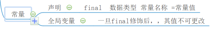
Variables, constants, operators

Detailed explanation on the use of annotation tool via (VGg image annotator) in mask RCNN

Network principle | connection management mechanism in TCP / IP important protocol and core mechanism
![[AI vision · quick review of NLP natural language processing papers today, issue 30] Thu, 14 APR 2022](/img/cc/21b20f56a7eb3e43b9c23792c597ef.png)
[AI vision · quick review of NLP natural language processing papers today, issue 30] Thu, 14 APR 2022
STM32上μC/Shell移植与应用
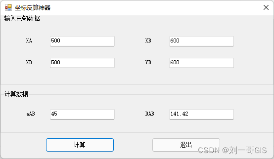
【测绘程序设计】坐标反算神器V1.0(附C/C#/VB源程序)
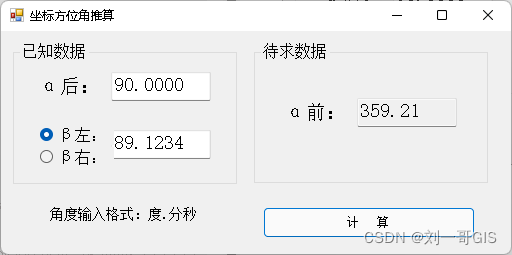
【测绘程序设计】坐标方位角推算神器(C#版)

ROS series (IV): ROS communication mechanism series (2): Service Communication
Writing latex with vscode - the latest tutorial 2022 / 4 / 17
随机推荐
Photoshop installation under win10
Paddlepaddle does not support arm64 architecture.
STM32F4单片机ADC采样及ARM-DSP库的FFT
How Zotero quotes in word jump to references / hyperlink
阿里云IoT流转到postgresql数据库方案
C language character constant
Does China Mobile earn 285 million a day? In fact, 5g is difficult to bring more profits, so where is the money?
[AI vision · quick review of NLP natural language processing papers today, issue 30] Thu, 14 APR 2022
Counting and sorting (C language implementation) -- learning notes
Vs Studio modifie le langage C scanf et d'autres erreurs
Software testing process
Raspberry pie 3B logs into the wired end of Ruijie campus network through mentohust, creates WiFi (open hotspot) for other devices, and realizes self startup at the same time
Opencv4 QR code recognition test
ROS series (IV): ROS communication mechanism series (3): parameter server
Variables, constants, operators
【ICCV 2019】MAP-VAE:Multi-Angle Point Cloud-VAE: Unsupervised Feature Learning for 3D Point Clouds..
UDP protocol and TCP protocol
Set经典小题目
Overview of knowledge map (II)
作为一名码农,女友比自己更能码是一种什么体验?