当前位置:网站首页>Switching power supply design sharing and power supply design skills diagram
Switching power supply design sharing and power supply design skills diagram
2022-04-23 19:01:00 【Reflection electron】
Start with the design and production process of switching power supply , Let's talk about the design of printed board first . Switching power supply operates at high frequency , High pulse state , It belongs to a special kind of analog circuit . The wiring principle of high-frequency circuit must be followed during board layout .
1、 Layout : The impulse voltage connection shall be as short as possible , The input switch tube is connected to the transformer , The output transformer is connected to the rectifier tube Line . The pulse current loop should be as small as possible, such as the positive input filter capacitance to the negative return capacitance from the transformer to the switch tube . The output part is from the output end of the transformer to the rectifier tube to the output inductance to the output capacitance and returns to the transformer circuit X The capacitor should be connected as far as possible Near the input of switching power supply , The input line should avoid parallel with other circuits , Avoid . Y The capacitor shall be placed at the grounding terminal of the casing or FG Connecting end . Common touch electric induction keeps a certain distance from the transformer , To avoid magnetic coupling . If it is difficult to handle, a shield can be added between the common touch inductor and the transformer , The above items are important for switching power supply The source of EMC High performance impact .
Generally, two output capacitors can be used, one close to the rectifier and the other close to the output terminal , It can affect the output ripple index of the power supply , The parallel connection effect of two small capacity capacitors should be better than that of one large capacity capacitor . Heating devices shall be connected with electrolysis Keep the capacitor at a certain distance , To prolong the service life of the whole machine , Electrolytic capacitor is the key to the life of switching power supply , Such as transformer 、 Power tube 、 High power resistors should keep a distance from electrolysis , Heat dissipation space must also be reserved between electrolytes , Conditions permit It can be placed at the air inlet .
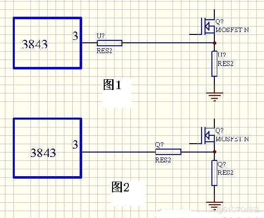
The control part should pay attention to : The wiring of high impedance weak signal circuit shall be as short as possible, such as sampling feedback loop , Try to avoid interference when handling 、 Current sampling signal circuit , Especially the current control circuit , If it's not handled well, it's easy to Some unexpected accidents , There are some techniques , Now 3843 An example of the circuit is shown in Figure (1) The effect of Figure 1 is better than that of Figure 2 , Fig. 2 obvious superimposed spikes on the current waveform observed by oscilloscope under full load , Current limiting due to interference The point is lower than the design value , There is no such phenomenon in Figure 1 、 There is also a switch tube drive signal circuit , The driving resistance of the switch tube shall be close to the switch tube , It can improve the working reliability of the switch tube , This has nothing to do with power MOSFET High DC impedance is related to voltage driving characteristics .
Let's talk about some principles of printed board wiring .
Line spacing : With the continuous improvement and improvement of printed circuit board manufacturing technology , Generally, the spacing of outgoing lines manufactured by processing plants is equal to or even less than 0.1mm There are no more problems , It can fully meet most applications . consider To the components and production process adopted by switching power supply , Generally, the minimum line spacing of double-sided board is set as 0.3mm, The minimum line spacing of single panel is set to 0.5mm, Pads and pads 、 Pad and via or via and via , Minimum The spacing is set to 0.5mm, It can avoid... During welding operation “ The bridge ” The phenomenon ., In this way, most plate factories can easily meet the production requirements , And can control the yield very high , It can also achieve reasonable There is an economical density of wiring .
The minimum line spacing is only suitable for signal control circuits and voltages below 63V Low voltage circuit , When the voltage between lines is greater than this value, it can generally be calculated according to 500V/1mm The empirical value takes the line spacing .
In view of some relevant standards, there are clear provisions on line spacing , We should strictly follow the standards , For example, the connection from the AC inlet end to the fuse end . Some power supplies require high volume , Such as module power supply . General transformer input The distance between side lines is 1mm Practice has proved that it is feasible . For AC input ,( Isolation ) Output of DC power supply , It is strictly stipulated that the safety distance shall be greater than or equal to 6mm, Of course, this depends on the relevant standards and implementation methods determine . The general safety distance can be referred to by the distance between both sides of the feedback optocoupler , The principle is greater than or equal to this distance . It can also be slotted on the printed board under the optocoupler , Increase the creepage distance to meet the insulation requirements . General switching power supply AC The wiring at the input side or the distance between the components on the board and the uninsulated shell 、 The radiator spacing shall be greater than 5mm, The distance between the output side wiring or device and the shell or radiator shall be greater than 2mm, Or strictly follow the safety specifications .
Common methods : The circuit board slotting method mentioned above is suitable for some occasions with insufficient spacing , By the way , This method is also commonly used as a protective discharge gap , It is common in the tail plate of TV picture tube and the AC input of power supply . This method has been widely used in modular power supply , Good results can be obtained under the condition of potting .
Method 2 : Pad insulating paper , Green shell paper can be used 、 Polyester film 、 PTFE directional film and other insulating materials . The general power supply is padded between the circuit board and the metal casing with green paper or polyester film , This material has high mechanical strength , Yes Have a certain ability to resist moisture . Polytetrafluoroethylene directional membrane is widely used in module power supply because of its high temperature resistance . An insulating film can also be padded between the element and the surrounding conductor to improve the electrical resistance of the insulation .
Be careful : The insulating cover of some devices cannot be used as insulating medium to reduce the safety distance , Such as the outer skin of electrolytic capacitor , At high temperatures , The skin may shrink under heat . Space shall be reserved at the front end of the large electrolytic explosion-proof tank , In order to ensure that the electrolytic capacitor can discharge voltage without obstruction under extraordinary circumstances .
Mr. Bai Jilong has been engaged in the electronics industry for 15 A year ,
So far, more than 100 products have been developed , At present, most of them have been mass-produced and listed ,
from 2018 It began to take 5 Years of time ,
Thousands of practical electronic engineer courses have been recorded with great concentration ,
The course ranges from components to core modules to complete products
Lao Bai's original intention is “ May engineers all over the world No detours ”
among ,
There are detailed explanations MOS Tube and IGBT Curriculum
版权声明
本文为[Reflection electron]所创,转载请带上原文链接,感谢
https://yzsam.com/2022/04/202204231844445143.html
边栏推荐
- ESP32 LVGL8. 1 - input devices (input devices 18)
- ctfshow-web361(SSTI)
- Circuit on-line simulation
- Configure iptables
- Advanced transfer learning
- #yyds干货盘点#stringprep --- 因特网字符串预备
- 电路在线模拟
- ESP32 LVGL8. 1. Detailed migration tutorial of m5stack + lvgl + IDF (27)
- Coolweather is revised and connected to the wind weather interface to realize the broken line diagram of temperature
- The type initializer for ‘Gdip‘ threw an exception
猜你喜欢
![[popular science] CRC verification (I) what is CRC verification?](/img/80/a1fa10ce6781aebf1b53d91fba52f4.png)
[popular science] CRC verification (I) what is CRC verification?
Machine learning practice - naive Bayes

Client interns of a large factory share their experience face to face
c#:泛型反射
Introduction to micro build low code zero Foundation (lesson 3)
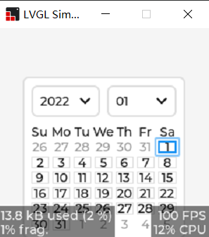
ESP32 LVGL8. 1 - calendar (calendar 25)
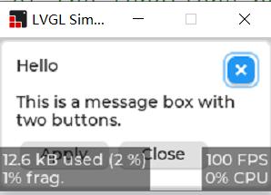
ESP32 LVGL8. 1 - msgbox message box (msgbox 28)
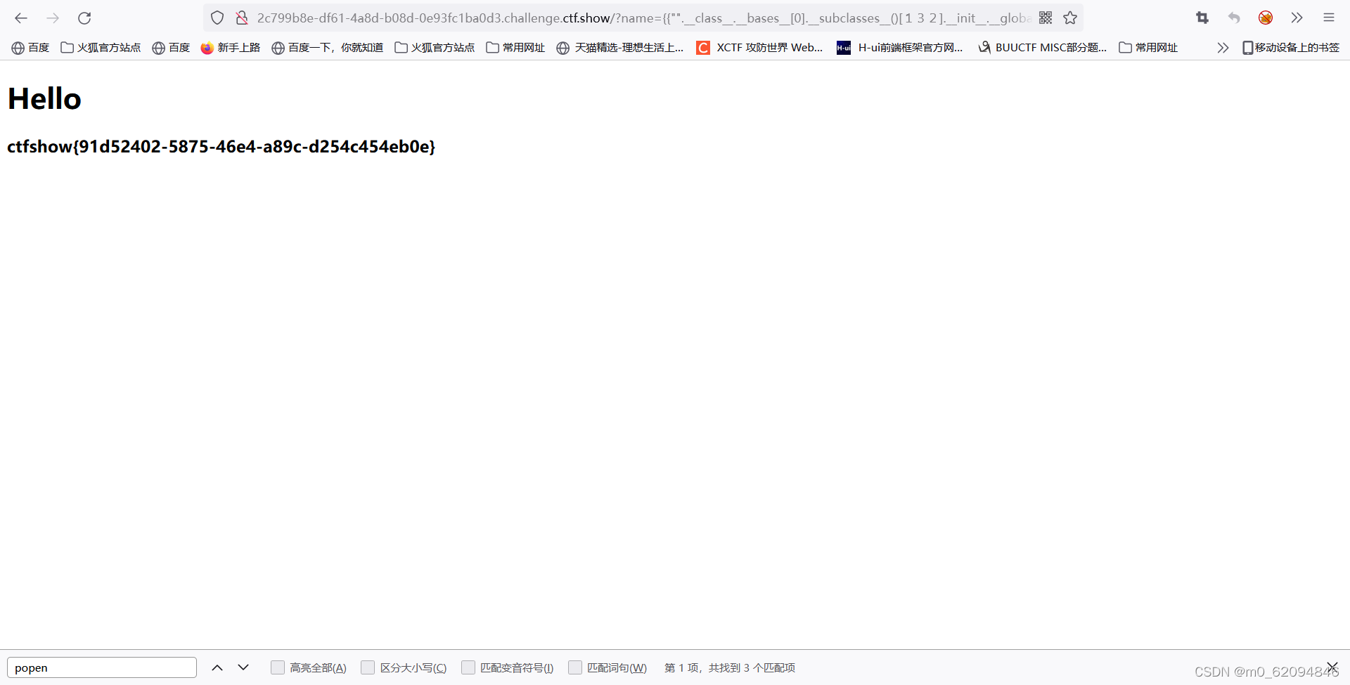
ctfshow-web362(SSTI)
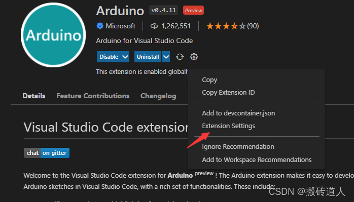
Using Visual Studio code to develop Arduino

Machine learning theory (8): model integration ensemble learning
随机推荐
Using Visual Studio code to develop Arduino
Xlslib use
mysql_linux版本的下載及安裝詳解
8266 obtain 18b20 temperature
关于unity文件读取的操作(一)
SSDB基础1
【玩转Lighthouse】腾讯云轻量服务器搭建全平台视频解析视频下载网站
实战业务优化方案总结---主目录---持续更新
22 year flying Book manpower Kit
mysql_ Download and installation of Linux version
Usage of functions decode() and replace() in SQL
Nacos cluster construction and MySQL persistence configuration
ESP32 LVGL8. 1 - msgbox message box (msgbox 28)
Esp32 (UART receiving and sending) - receiving and sending communication of serial port (4)
Teach you to quickly rename folder names in a few simple steps
The fifth bullet of MySQL learning -- detailed explanation of transaction and its operation characteristics
Raspberry pie 18b20 temperature
Nacos as service registry
Machine learning theory (8): model integration ensemble learning
Esp01s with Arduino development environment