当前位置:网站首页>STM32: LCD display
STM32: LCD display
2022-04-23 18:33:00 【Xi Wu Wen Lu】
One 、TFTLCD summary
1.1 TFTLCD
TFT-LCD Thin film transistor liquid crystal display . Its full English name is :Thin Film Transistor-Liquid Crystal
Display, The module has the following features :
- 2.4’、2.8’、3.5’、4.3’、7’, 5 Screen sizes are available ;
- 320×240 The resolution of the (3.5’ A resolution of :320*480,4.3’ and 7’ A resolution of :800*480)
- 16 Bit true color shows .
- With touch screen , Can be used as control input .
This article takes 2.8 Inch screen as an example , To introduce .2.8 The display resolution of inch screen is 320x240, Interface for 16 Bit 80 In parallel , With touch screen .

1.2 TFTLCD Interface
TFTLCD Module adoption 2*17 Of 2.54 Pin and external connection , The interface is defined as follows :
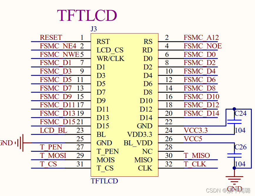
Pictured above , It can be seen that ,TFTLCD use 16 Bit Union and external connection , Why not use 8 The way of bit , Because of the large amount of data on the color screen , Especially when showing pictures , If you use 8 Bit data line , It will be better than 16 Bit mode is more than twice as slow , Of course we want to be as fast as possible , So we choose 16 Bit interface .
except 80 Outside the parallel port data line , The module also has some The signal line :
- RST: Hard reset TFTLCD
- CS:TFTLCD Piece of optional signal
- RS: command / Data signs (0, Read and write commands [ Control register ];1, Read and write data [ Data register ])
- WR: towards TFTLCD Write data
- RD: from TFTLCD Reading data
- D[15:0]:16 Bit bidirectional data line
TFTLCD There are many kinds of driver chips for modules , This article takes ILI9341 For example, controller , To introduce .ILI9341 Self storage LCD controller , The total memory size is 172800(240*320*18/8) byte , namely 18 Bit mode (26 Ten thousand colors ) The amount of video memory under . stay 16 In bit mode ,ILI9341 use RGB565 Format to store color data , here ILI9341 Of 18 Bit data line and MCU Of 16 Bit data lines and LCD GRAM As shown in the figure :
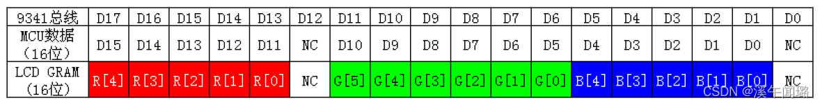
As you can see from the diagram ,ILI9341 stay 16 In bit mode , What's useful about data lines is :D17~D13 and D11~D1,D0 and D12 Not used , In fact, in us LCD Inside the module ,ILI9341 Of D0 and D12 It didn't come out at all , such ,ILI9341 Of D17~D13 and D11~D1 Corresponding MCU Of D15~D0.
such MCU Of 16 Bit data , The minimum 5 Blue , middle 6 Bit green , The highest 5 Bits are red . The higher the value is
Big , The darker the color is . in addition , Particular attention ILI9341 All the instructions are 8 Bit ( high 8 Bit invalid ), And parameters Except for reading and writing GRAM The time is 16 position , Other operating parameters , All are 8 Bit .
1.3 ILI9341 Instructions
1.3.1 0XD3 Instructions
Instructions 0XD3 One is reading ID4 Instructions , For reading LCD Controller ID, The instruction is shown in the following table :

As can be seen from the table above ,0XD3 The command was followed by 4 Parameters , Last 2 Parameters , Read it out to be 0X93 and 0X41, It happens to be our controller ILI9341 The digital part of , thus , By this instruction , Can be used to determine the use of LCD What type of drive is , such , Our code , According to the model of the controller, the corresponding driver can be executed IC Initialization code , So as to be compatible with different drivers IC Screen of , Make one code support multiple LCD.
1.3.2 0X36 Instructions
0X36 Instructions are stored access control instructions , Can be controlled ILI9341 Read and write direction of memory , To put it simply , It's just continuous writing GRAM When , Can be controlled GRAM The growth direction of the pointer , So as to control the display mode ( read GRAM Is the same ). The instruction is shown in the following table :
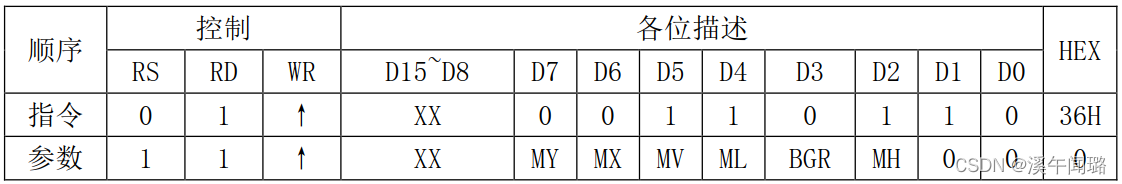
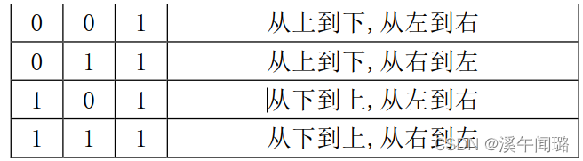
As can be seen from the table above ,0X36 After instruction , It's followed by a parameter , Here we focus on :MY、MX、MV These three people , By setting these three bits , We can control the whole thing ILI9341 All scanning directions of , As shown in the following table :

such , We're using ILI9341 When the content is displayed , There's a lot of flexibility .
1.3.3 0X2A Instructions
0X2A Is the column address setting instruction , From left to right , Scanning from top to bottom ( Default ) below , This command is used to set the abscissa (x coordinate ), The instruction is shown in the table :

In Default scan mode , This command is used to set x coordinate , The instruction carries 4 Parameters , It's actually 2 Coordinates :SC and EC, The starting and ending values of the column address ,SC Must be less than or equal to EC, And 0≤SC/EC≤239. It's usually set x When it comes to coordinates , We just need to bring 2 Just one parameter , That is, setting SC that will do , Because if EC There is no change , We need to set it once ( Initializing ILI9341 When setting ), To speed up .
1.3.4 0X2B Instructions
And 0X2A Instruction similar , Instructions :0X2B, Is the page address setting instruction , From left to right , Scanning from top to bottom ( Default ) below , This command is used to set the ordinate (y coordinate ).

In Default scan mode , This command is used to set y coordinate , The instruction carries 4 Parameters , It's actually 2 Coordinates :SP and EP, The starting and ending values of the page address ,SP Must be less than or equal to EP, And 0≤SP/EP≤319, It's usually set
y When it comes to coordinates , We just need to bring 2 Just one parameter , That is, setting SP that will do , Because if EP There is no change , I
You only need to set it once ( Initializing ILI9341 When setting ), To speed up .
1.3.5 0X2C Instructions
0X2C The instruction is to write GRAM Instructions , After sending the command , We can go to LCD Of GRAM Color data is written in it , The instruction supports continuous writing , The instructions are described in the following table :


It can be seen from the above table that , After receiving instructions 0X2C after , The data effective bit width becomes 16 position , We can write continuously LCD
GRAM value , and GRAM The address of will be based on MY/MX/MV Set the scanning direction to increase automatically . for example : Suppose you set it from left to right , Scanning from top to bottom , So set the starting coordinates ( adopt SC,SP Set up ) after , Every time a color value is written ,GRAM The address will automatically increase 1(SC++), If you come across EC, Then go back to SC, meanwhile SP++, All the way to the coordinates :EC,EP end , Coordinates that do not need to be set again , This greatly improves the writing speed .
1.3.6 0X2E Instructions
0X2E The instruction is read GRAM Instructions , For reading ILI9341 Explicit memory of (GRAM), As shown in the following table :
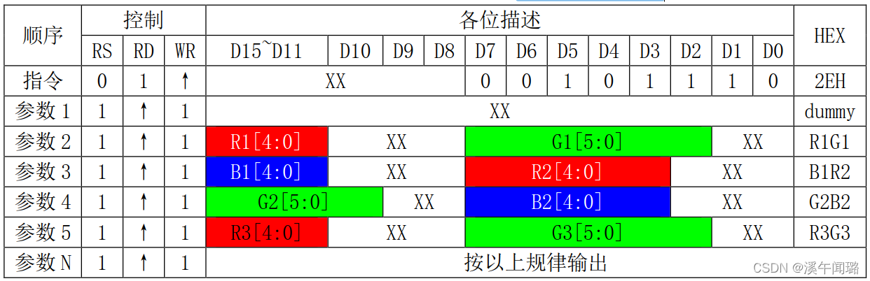
This instruction is used to read GRAM, As shown in the table above ,ILI9341 After receiving the order , The first output is dummy data , That is, invalid data , The second time starts , What is read is valid GRAM data ( From coordinates :SC,SP Start ), The output law is : Each color component accounts for 8 bits , One output 2 Color components . such as : The first output is R1G1, The law that follows is :B1R2-G2B2-R3G3-B3R4-G4B4-R5G5... And so on . If we just need to read the color value of a point , Then you just need to receive the parameters 3 that will do , If you want to read continuously ( utilize GRAM Address auto increment , Method is the same as above. ), Then according to the above rules to receive color data .
1.4 TFTLCD Usage flow :
commonly TFTLCD The use flow of the module is shown in the following figure :

whatever LCD, The flow chart above can be used to show the flow chart . The hard reset and initialization sequence , It only needs to be executed once . And the process of drawing is : Set coordinates --> Write GRAM Instructions --> Write color data , And then in LCD On
Noodles , We can see that the corresponding dot shows the color we wrote . The reading process is : Set coordinates --> read GRAM Instructions
--> Read color data , In this way, we can get the color data of the corresponding points .
1.5 TFTLCD Display setup steps
- Set up STM32F4 And TFTLCD Modules connected to each other IO.
This step , First we will be with TFTLCD Module connected IO The port is initialized , In order to drive LCD. What we use here is FSMC.
- initialization TFTLCD modular .
The initialization steps are as follows: 1.4 The initialization sequence shown in the figure , Initialization sequence , That is to say LCD The controller writes a series of settings ( Like gamma calibration ), These initialization sequences are generally LCD The supplier will provide to the customer , We can use these sequences directly , No further research is needed . After initialization ,LCD Can be used normally .
- Display characters and numbers to TFTLCD On module
This step is through 1.4 The process on the left , namely : Set coordinates --> Write GRAM Instructions --> Write GRAM To achieve , But this step , It's just a point processing , We want to display characters / Numbers , You have to use this step multiple times , So as to display characters / The purpose of numbers .
Two 、FSMC summary
FSMC, That is, flexible Static storage controller , Ability to work with synchronous or asynchronous storage and 16 position PC Memory card connection ,STM32F4 Of FSMC Interface support includes SRAM、NAND FLASH、NOR FLASH and PSRAM Equal storage .FSMC The block diagram of is shown in the figure below :

As you can see from the diagram ,FSMC Divide external devices into two categories ,NOR/PSRAM equipment 、NAND/PC Card equipment .LCD Is regarded as SRAM Controlled .
FSMC Drive external SRAM when , external SRAM In general, there are : Address line ( Such as A0~A25)、 cable ( Such as D0~D15)、 Write the signal (WE, namely WR)、 Read the signal (OE, namely RD)、 Piece of optional signal (CS), If SRAM Support byte control , Then there are UB/LB The signal .
Introducing TFTLCD When , Introduced its interface , Yes RS、D0~D15、WR、RD、CS, Its operation sequence and SRAM It's very similar to , The only difference is TFTLCK Yes RS The signal , And no address signal .
TFTLCD adopt RS Signal to determine whether the transmitted data is data or command , In essence, it can be understood as an address letter
Number , For example, we put RS Connect to A0 above , So when FSMC The controller writes the address 0 When , Will make A0 Turn into 0, Yes TFTLCD Come on , It's about writing orders . and FSMC Write the address 1 When ,A0 It will become 1, Yes TFTLCD Come on , It's about writing data . such , It separates data from command , They are actually corresponding to SRAM Two consecutive addresses of the operation .
therefore , You can put TFTLCD Think of it as a SRAM To use , It's just this SRAM Only two addresses , This is it. FSMC drive LDC Principle .
STM32 Of FSMC Support 8、16、32 Bit data width , What we use here is 16 position , because LCD yes 16 The width of the bit .FSMC Divide external memory into fixed sizes of 256M Four memory blocks of bytes , As shown in the figure below :

As can be seen from the above figure ,FSMC Manage... In total 1GB Space , Have 4 Storage blocks (Bank), So here's what we're going to use SRAM That is, a block 1.FSMC Memory block 1(Bank1) Divided into 4 Districts , Each zone manages 64M Byte space , Each area has an independent register to configure the connected memory .Bank1 Of 256M Byte space is made up of 28 Root address line (HADDR[27:0]) Addressing .
here HADDR It's internal AHB Address bus , among HADDR[25:0] From external memory address FSMC_A[25:0], and HADDR[26:27] Yes 4 The address of each area , As shown in the following table :

When Bank1 The next thing is 16 Bit width memory :HADDR[25:1]-->FSMC_A[24:0].
When Bank1 The next thing is 8 Bit width memory :HADDR[25:0]--> FSMC_A[25:0]
Regardless of the external connection 8 position /16 Bit width devices ,FSMC_A[0] Always connect to the external device address A[0].
The data bit width here is important . Here HADDR Is addressed in bytes , And our external memory does not necessarily follow 8 Bit byte addressing , therefore , Depending on the memory data width , The address actually sent to the memory will also be different . Here's the picture :

When the memory width is 8 When a , That door coincides with HADDR Corresponding to the rule of byte addressing , That is to say 8 A byte address ,HADDR Address A0~A25 Have been used to . The maximum capacity that memory can have is ,64MB(A0~A25 The address represents at most 64MB Address )*8bit = 512Mb.
however , When the memory data width is 16 When a , At this time , For the same 512Mb Storage space , The required address is 512Mb/16bit = 32MB, and A0~A25 It can be represented 64MB Of the address of , therefore , When the data bit width is 16 When a , The address bits actually used are HADDR[25:1], namely no need HADDR[0] position , That's just right 32Mb, But each address has 16 Bit data , So the memory capacity is still 64MB/2 * 16 = 512Mb. The real operation is , Will move the address bit one bit to the right , namely HADDR[1] Corresponding A[0], and HADDR[25] Corresponding A[24]. This also guarantees , Even if the data bit width is 16 position ,FSMC_A[0] It's still the address of the external device A[0].
With A12 Pick up RS Line to analyze :A12 Pick up RS Line , When the command is operated A12 Should be 0, here FSMC_A The binary representation of the address is :0 1111 1111 1111, in other words ,HADDR[1] Corresponding A[0], and HADDR[0] no need , by 0, The binary representation of its address is :01 1111 1111 1110, Convert to 16 Hexadecimal is 0X1FFE. and RS by 1, That's the next address , It represents data operation , At this time , Just give it before 0X1FFE+0X02, That's all right. , The reason to add 2, Because the memory is 16 Bit , Its next address spans 16 Bit data , and HADDR In order to 8 Bit addressable , So its address should be added 2. That is to say 0x2000.
Two 、 software design
2.1 LCD.H file :
/
//LCD Hardware parameters
typedef struct
{
	u16 width;			//LCD  Width  320
	u16 height;			//LCD  Height  640
	u16 id;				//LCD ID
	u8  dir;			// Horizontal screen or vertical screen : 0  Streamer ,1  Vertical screen
	u16	 wramcmd;		// Start writing GRAM Instructions
	u16  setxcmd;		// Set up x Coordinate command
	u16  setycmd;		// Set up y Coordinate command
}_lcd_dev;

//LCD Parameters
extern _lcd_dev lcddev;	// management LCD Important parameter
//LCD  Brush color and background color
extern u16  POINT_COLOR;
extern u16  BACK_COLOR;

//-----------------LCD Backlight port definition ----------------
#define	LCD_BACK PFout(10)  //LCD Backlight     	PF10


// A12(RS)  As a data command line
// RS The line is used to decide whether to transmit data or commands .
//  Because here FSMC drive LCD The use of NOR/SRAM Of Bank1 Of sector4, Its base address is 0x6C000000
//  and A12 Divide lines for data commands , It represents an offset of 0x00001FFE,
//  analysis :0X00001FFE Change to binary to 1 1111 1111 1110,16 Bit address , Move the address one bit to the right ,
//  That is to say 0 1111 1111 1111; This is just the first 12 position A12 by 0.
//       however , If 16 Bit address plus 1( Corresponding to 8 Bit address is plus 2, namely 0x00001FFE+0x02),
//  That is to say 0x00002000, namely 1 0000 0000 0000
//       here ,A12 Namely 1, That is to say, right RS Of 0 and 1 control .
#define  CMD_BASE     ((u32)(0x6C000000 | 0x00001FFE))     //0x00001FFE Is the offset from the base address
#define  DATA_BASE    ((u32)(0x6C000000 | 0x00002000))

#define LCD_CMD       ( * (u16 *) CMD_BASE )      // here RS==0
#define LCD_DATA      ( * (u16 *) DATA_BASE)      // here RS==1

// Scan direction definition
#define  L2R_U2D  0 // From left to right , From top to bottom
#define  L2R_D2U  1 // From left to right , From bottom to top
#define  R2L_U2D  2 // From right to left , From top to bottom
#define  R2L_D2U  3 // From right to left , From bottom to top

#define  U2D_L2R  4 //  From top to bottom , From left to right
#define  U2D_R2L  5 //  From bottom to top , From left to right
#define  D2U_L2R  6 //  From top to bottom , From right to left
#define  D2U_R2L  7 //  From bottom to top , From right to left


//  Color definition
#define  WHITE        0xFFFF
#define  BLACK        0x0000
#define  RED          0xF800
#define  GREEN        0x07E0
#define  BLUE         0x001F
#define  BRED         0XF81F
#define  GRED 			  0XFFE0
#define  GBLUE			  0X07FF
#define  BROWN 			  0XBC40
#define  BRRED 			  0XFC07
#define  GRAY  			  0X8430
#define  MAGENTA      0xF81F
#define  CYAN         0x7FFF
#define  YELLOW       0xFFE0

void LCD_WriteReg(u16 LCD_Reg, u16 LCD_Value);
u16 LCD_ReadReg(u16 LCD_Reg);
void LCD_WriteGRAM(void);

void LCD_Init(void);				                // initialization
void LCD_DisplayOn(void);							// Turn on the display
void LCD_DisplayOff(void);							// Turn off the display
void LCD_Clear(u16 Color);	 						// Clear the screen
void LCD_SetCursor(u16 Xpos, u16 Ypos);				// Set the cursor
void LCD_DrawPoint(u16 x,u16 y);					// Draw a dot
void LCD_Color_DrawPoint(u16 x,u16 y,u16 color);	// Color dot
u16  LCD_GetPoint(u16 x,u16 y); 					// To read some

void LCD_Open_Window(u16 X0,u16 Y0,u16 width,u16 height);
void Set_Scan_Direction(u8 direction);
void Set_Display_Mode(u8 mode);

void LCD_Fill_onecolor(u16 sx,u16 sy,u16 ex,u16 ey,u16 color);		// Fill a single color
void LCD_Draw_Picture(u16 sx,u16 sy,u16 ex,u16 ey,u16 *color);		// Fill the specified color
void LCD_DisplayChar(u16 x,u16 y,u8 word,u8 size);					// Display a character
void LCD_DisplayString(u16 x,u16 y,u8 size,u8 *p);		            // Display a 12/16/24 Font string
void LCD_DisplayString_color(u16 x,u16 y,u8 size,u8 *p,u16 brushcolor,u16 backcolor); // Display a 12/16/24 Font custom color string
void LCD_DisplayNum(u16 x,u16 y,u32 num,u8 len,u8 size,u8 mode);	// Show numbers
void LCD_DisplayNum_color(u16 x,u16 y,u32 num,u8 len,u8 size,u8 mode,u16 brushcolor,u16 backcolor); // Display custom color numbers
2.2 LCD.C The file is introduced :
Hardware connection , We use FSMC Of Bank1 To control TFTLCD, The procedure flow is as follows :
- initialization TFTLCD Corresponding GPIO mouth , Initialization FSMC
- TFTLCD initialization , Contains the initialization sequence
- To write TFTLCD Show function
2.1.1 FSMC initialization :
// To configure FSMC
void LCD_FSMC_Config()
{
	GPIO_InitTypeDef  GPIO_InitStructure;
	FSMC_NORSRAMInitTypeDef  FSMC_NORSRAMInitStructure;
    FSMC_NORSRAMTimingInitTypeDef  readWriteTiming;
	FSMC_NORSRAMTimingInitTypeDef  writeTiming;

	RCC_AHB1PeriphClockCmd(RCC_AHB1Periph_GPIOD|RCC_AHB1Periph_GPIOE|RCC_AHB1Periph_GPIOF|RCC_AHB1Periph_GPIOG, ENABLE);
  RCC_AHB3PeriphClockCmd(RCC_AHB3Periph_FSMC,ENABLE);// Can make FSMC The clock

	GPIO_InitStructure.GPIO_Pin = GPIO_Pin_10;        //PF10  Push pull output , Control backlight
  GPIO_InitStructure.GPIO_Mode = GPIO_Mode_OUT;     // The output mode
  GPIO_InitStructure.GPIO_OType = GPIO_OType_PP;    // Push pull output
  GPIO_InitStructure.GPIO_Speed = GPIO_Speed_50MHz; //100MHz
  GPIO_InitStructure.GPIO_PuPd = GPIO_PuPd_UP;      // Pull up
  GPIO_Init(GPIOF, &GPIO_InitStructure);            // initialization PF10

  GPIO_InitStructure.GPIO_Pin = (3<<0)|(3<<4)|(7<<8)|(3<<14);
  GPIO_InitStructure.GPIO_Mode = GPIO_Mode_AF;      // Reuse output
  GPIO_InitStructure.GPIO_OType = GPIO_OType_PP;    // Push pull output
  GPIO_InitStructure.GPIO_Speed = GPIO_Speed_100MHz;//100MHz
  GPIO_InitStructure.GPIO_PuPd = GPIO_PuPd_UP;      // Pull up
  GPIO_Init(GPIOD, &GPIO_InitStructure);            // initialization

  GPIO_InitStructure.GPIO_Pin = (0X1FF<<7);         //PE7~15,AF OUT
  GPIO_InitStructure.GPIO_Mode = GPIO_Mode_AF;      // Reuse output
  GPIO_InitStructure.GPIO_OType = GPIO_OType_PP;    // Push pull output
  GPIO_InitStructure.GPIO_Speed = GPIO_Speed_100MHz;//100MHz
  GPIO_InitStructure.GPIO_PuPd = GPIO_PuPd_UP;      // Pull up
  GPIO_Init(GPIOE, &GPIO_InitStructure);            // initialization

	GPIO_InitStructure.GPIO_Pin = GPIO_Pin_2;         //PG2
  GPIO_InitStructure.GPIO_Mode = GPIO_Mode_AF;      // Reuse output
  GPIO_InitStructure.GPIO_OType = GPIO_OType_PP;    // Push pull output
  GPIO_InitStructure.GPIO_Speed = GPIO_Speed_100MHz;//100MHz
  GPIO_InitStructure.GPIO_PuPd = GPIO_PuPd_UP;      // Pull up
  GPIO_Init(GPIOG, &GPIO_InitStructure);            // initialization

	GPIO_InitStructure.GPIO_Pin = GPIO_Pin_12;        //PG12
  GPIO_InitStructure.GPIO_Mode = GPIO_Mode_AF;      // Reuse output
  GPIO_InitStructure.GPIO_OType = GPIO_OType_PP;    // Push pull output
  GPIO_InitStructure.GPIO_Speed = GPIO_Speed_100MHz;//100MHz
  GPIO_InitStructure.GPIO_PuPd = GPIO_PuPd_UP;      // Pull up
  GPIO_Init(GPIOG, &GPIO_InitStructure);            // initialization

  GPIO_PinAFConfig(GPIOD,GPIO_PinSource0,GPIO_AF_FSMC);
  GPIO_PinAFConfig(GPIOD,GPIO_PinSource1,GPIO_AF_FSMC);
  GPIO_PinAFConfig(GPIOD,GPIO_PinSource4,GPIO_AF_FSMC);
  GPIO_PinAFConfig(GPIOD,GPIO_PinSource5,GPIO_AF_FSMC);
  GPIO_PinAFConfig(GPIOD,GPIO_PinSource8,GPIO_AF_FSMC);
  GPIO_PinAFConfig(GPIOD,GPIO_PinSource9,GPIO_AF_FSMC);
  GPIO_PinAFConfig(GPIOD,GPIO_PinSource10,GPIO_AF_FSMC);
  GPIO_PinAFConfig(GPIOD,GPIO_PinSource14,GPIO_AF_FSMC);
  GPIO_PinAFConfig(GPIOD,GPIO_PinSource15,GPIO_AF_FSMC);

  GPIO_PinAFConfig(GPIOE,GPIO_PinSource7,GPIO_AF_FSMC);
  GPIO_PinAFConfig(GPIOE,GPIO_PinSource8,GPIO_AF_FSMC);
  GPIO_PinAFConfig(GPIOE,GPIO_PinSource9,GPIO_AF_FSMC);
  GPIO_PinAFConfig(GPIOE,GPIO_PinSource10,GPIO_AF_FSMC);
  GPIO_PinAFConfig(GPIOE,GPIO_PinSource11,GPIO_AF_FSMC);
  GPIO_PinAFConfig(GPIOE,GPIO_PinSource12,GPIO_AF_FSMC);
  GPIO_PinAFConfig(GPIOE,GPIO_PinSource13,GPIO_AF_FSMC);
  GPIO_PinAFConfig(GPIOE,GPIO_PinSource14,GPIO_AF_FSMC);
  GPIO_PinAFConfig(GPIOE,GPIO_PinSource15,GPIO_AF_FSMC);

  GPIO_PinAFConfig(GPIOG,GPIO_PinSource2,GPIO_AF_FSMC);
  GPIO_PinAFConfig(GPIOG,GPIO_PinSource12,GPIO_AF_FSMC);

  readWriteTiming.FSMC_AddressSetupTime = 0XF;	 // Address establishment time (ADDSET) 16 individual HCLK 1/168M=6ns*16=96ns
  readWriteTiming.FSMC_AddressHoldTime = 0x00;	 // Address hold time (ADDHLD)
  readWriteTiming.FSMC_DataSetupTime = 60;			 // Data storage time  60 individual HCLK	= 6*60=360ns
  readWriteTiming.FSMC_BusTurnAroundDuration = 0x00;
  readWriteTiming.FSMC_CLKDivision = 0x00;
  readWriteTiming.FSMC_DataLatency = 0x00;
  readWriteTiming.FSMC_AccessMode = FSMC_AccessMode_A;

	writeTiming.FSMC_AddressSetupTime =8;	     // Address establishment time (ADDSET)9 individual HCLK =54ns
  writeTiming.FSMC_AddressHoldTime = 0x00;	 // Address hold time
  writeTiming.FSMC_DataSetupTime = 7;		     // Data storage time  6ns*9 individual HCLK=54ns
  writeTiming.FSMC_BusTurnAroundDuration = 0x00;
  writeTiming.FSMC_CLKDivision = 0x00;
  writeTiming.FSMC_DataLatency = 0x00;
  writeTiming.FSMC_AccessMode = FSMC_AccessMode_A;

  FSMC_NORSRAMInitStructure.FSMC_Bank = FSMC_Bank1_NORSRAM4;
  FSMC_NORSRAMInitStructure.FSMC_DataAddressMux = FSMC_DataAddressMux_Disable;
  FSMC_NORSRAMInitStructure.FSMC_MemoryType =FSMC_MemoryType_SRAM;
  FSMC_NORSRAMInitStructure.FSMC_MemoryDataWidth = FSMC_MemoryDataWidth_16b;   // Data width is 16bit
  FSMC_NORSRAMInitStructure.FSMC_BurstAccessMode =FSMC_BurstAccessMode_Disable;
  FSMC_NORSRAMInitStructure.FSMC_WaitSignalPolarity = FSMC_WaitSignalPolarity_Low;
	FSMC_NORSRAMInitStructure.FSMC_AsynchronousWait=FSMC_AsynchronousWait_Disable;
  FSMC_NORSRAMInitStructure.FSMC_WrapMode = FSMC_WrapMode_Disable;
  FSMC_NORSRAMInitStructure.FSMC_WaitSignalActive = FSMC_WaitSignalActive_BeforeWaitState;
  FSMC_NORSRAMInitStructure.FSMC_WriteOperation = FSMC_WriteOperation_Enable;	 // Write enable
  FSMC_NORSRAMInitStructure.FSMC_WaitSignal = FSMC_WaitSignal_Disable;
  FSMC_NORSRAMInitStructure.FSMC_ExtendedMode = FSMC_ExtendedMode_Enable;      // Reading and writing use different timing
  FSMC_NORSRAMInitStructure.FSMC_WriteBurst = FSMC_WriteBurst_Disable;
  FSMC_NORSRAMInitStructure.FSMC_ReadWriteTimingStruct = &readWriteTiming;     // Read write timing
  FSMC_NORSRAMInitStructure.FSMC_WriteTimingStruct = &writeTiming;             // Write timing
  FSMC_NORSRAMInit(&FSMC_NORSRAMInitStructure);  // initialization FSMC
  FSMC_NORSRAMCmd(FSMC_Bank1_NORSRAM4, ENABLE);  // Can make Bank1
  delay_ms(50);
}
2.1.2 Set up LCD Important parameter
Set up _lcd_dev Structure :
/****************************************************************************
* name call : void Set_Display_Mode(u8 mode)
* work can : Set up LCD Show direction
* Entrance parameters :mode: 0, Vertical screen
1, Horizontal screen
* Returns the parameter : nothing
* say bright :
****************************************************************************/
void Set_Display_Mode(u8 mode)
{
if(mode==0) // Vertical screen
{
lcddev.dir=0;
if(lcddev.id==0X9341)
{
lcddev.wramcmd=0X2C; //GRAM Instructions
lcddev.setxcmd=0X2A; // Write X Coordinate command
lcddev.setycmd=0X2B; // Write Y Coordinate command
lcddev.width=240; // Set width 240
lcddev.height=320; // Set height 320
}
else if(lcddev.id==0X1963)
{
lcddev.wramcmd=0X2C;
lcddev.setxcmd=0X2B;
lcddev.setycmd=0X2A;
lcddev.width=480;
lcddev.height=800;
}
}
else // Horizontal screen
{
lcddev.dir=1;
if(lcddev.id==0X9341)
{
lcddev.wramcmd=0X2C;
lcddev.setxcmd=0X2A;
lcddev.setycmd=0X2B;
lcddev.width=240;
lcddev.height=320;
}
else if(lcddev.id==0X1963)
{
lcddev.wramcmd=0X2C; //GRAM Instructions
lcddev.setxcmd=0X2B; // Write X Coordinate command
lcddev.setycmd=0X2A; // Write Y Coordinate command
lcddev.width=480; // Set width 480
lcddev.height=800; // Set height 800
}
}
Set_Scan_Direction(L2R_U2D); // Set scan direction From left to right , From bottom to top
} 2.1.3 Write register value
/****************************************************************************
*  name      call : void LCD_WriteReg(u16 LCD_Reg, u16 LCD_Value)
*  work      can :LCD Write register
*  Entrance parameters :LCD_Reg:  Register address
*           LCD_RegValue:  The data to be written
*  Returns the parameter : nothing
*  say      bright :
****************************************************************************/
void LCD_WriteReg(u16 LCD_Reg, u16 LCD_Value)
{
	LCD_CMD = LCD_Reg;		 // Write the serial number of the register to be written
	LCD_DATA = LCD_Value;  // Data written to the register
}
2.1.4 Write GRAM Instructions
// Start writing GRAM
//0X2c For writing GRAM Instructions . After sending the instruction , You can go to LCD Of GRAM Write color data .
void LCD_WriteGRAM(void)
{
 	LCD_CMD=lcddev.wramcmd;	  // 0X2C
}
2.1.5 Set cursor position
/****************************************************************************
*  name      call : void LCD_SetCursor(u16 Xaddr, u16 Yaddr)
*  work      can : Set cursor position
*  Entrance parameters :x:x coordinate
            y:y coordinate
*  Returns the parameter : nothing
*  say      bright :
****************************************************************************/
void LCD_SetCursor(u16 Xaddr, u16 Yaddr)
{
			LCD_CMD=lcddev.setxcmd;
			LCD_DATA=(Xaddr>>8);
			LCD_DATA=(Xaddr&0XFF);
			LCD_CMD=lcddev.setycmd;
			LCD_DATA=(Yaddr>>8);
			LCD_DATA=(Yaddr&0XFF);
}
2.1.6 Draw a dot
/****************************************************************************
* name call : void LCD_DrawPoint(u16 x,u16 y)
* work can : Draw a dot ( Write the color of the brush at this point )
* Entrance parameters :x:x coordinate
y:y coordinate
* Returns the parameter : nothing
* say bright RUSH_COLOR: The color value of this point
****************************************************************************/
void LCD_DrawPoint(u16 x,u16 y)
{
LCD_SetCursor(x,y); // Set cursor position
LCD_WriteGRAM(); // Start writing GRAM
LCD_DATA=POINT_COLOR;
}/****************************************************************************
* name call : void LCD_Color_DrawPoint(u16 x,u16 y,u16 color)
* work can : Draw the corresponding color at the set coordinates ( Write a custom color at this point )
* Entrance parameters :x:x coordinate
y:y coordinate
color The color value of this point
* Returns the parameter : nothing
* say bright :color: Write the color value of this point GUI Call this function
****************************************************************************/
void LCD_Color_DrawPoint(u16 x,u16 y,u16 color)
{
LCD_SetCursor(x,y); // Set cursor position
LCD_WriteGRAM(); // Start writing GRAM
LCD_DATA=color;
} 2.1.7 Screen clearing function
/****************************************************************************
* name call : void LCD_Clear(u16 color)
* work can : Screen clearing function
* Entrance parameters :color: Fill color to clear the screen
* Returns the parameter : nothing
* say bright :
****************************************************************************/
void LCD_Clear(u16 color)
{
u32 i=0;
u32 pointnum=0;
pointnum=lcddev.width*lcddev.height; // obtain LCD Total points
LCD_SetCursor(0x00,0x00); // Set cursor position
LCD_WriteGRAM(); // Start writing GRAM
for(i=0;i<pointnum;i++)
{
LCD_DATA=color;
}
}2.1.8 Read some color
/****************************************************************************
*  name      call : u16 LCD_GetPoint(u16 x,u16 y)
*  work      can : Read the color value of a point
*  Entrance parameters :x:x coordinate
            y:y coordinate
*  Returns the parameter : The color of this point
*  say      bright :
****************************************************************************/
u16 LCD_GetPoint(u16 x,u16 y)
{
 	vu16 r=0,g=0,b=0;

	LCD_SetCursor(x,y);

	LCD_CMD=0X2E;   //9341 And 1963 read GRAM The instructions are the same
	r=LCD_DATA;

 	if(lcddev.id==0X1963)
		 return r;		   //1963 Just read it out 16 Bit color value

	else	 // Other drivers are 9341
 	{
		 lcdm_delay(2);
		 b=LCD_DATA;    //9341 Read 2 Time
		 g=r&0XFF;		  //9341 The first read is RG Value ,R before ,G After , Each account 8 position
		 g<<=8;
		 return (((r>>11)<<11)|((g>>10)<<5)|(b>>11)); //9341 The formula needs to be converted
	}
}
3、 ... and 、 end
Engineering source :https://download.csdn.net/download/sssxlxwbwz/85205397
版权声明
本文为[Xi Wu Wen Lu]所创,转载请带上原文链接,感谢
https://yzsam.com/2022/04/202204231827369752.html
边栏推荐
- Notepad + + replaces tabs with spaces
- os_authent_prefix
- After CANopen starts PDO timing transmission, the heartbeat frame time is wrong, PDO is delayed, and CANopen time axis is disordered
- Introduction to QT programming
- Using transmittablethreadlocal to realize parameter cross thread transmission
- Closure type of rust (difference between FN, fnmut and fnone)
- Jeecg boot microservice architecture
- WiFi ap6212 driver transplantation and debugging analysis technical notes
- Daily CISSP certification common mistakes (April 11, 2022)
- SQL database syntax learning notes
猜你喜欢
机器学习理论之(7):核函数 Kernels —— 一种帮助 SVM 实现非线性化决策边界的方式
Robocode tutorial 7 - Radar locking
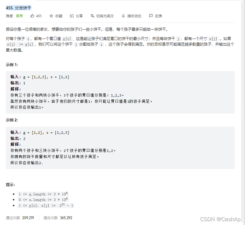
【ACM】455. Distribute Biscuits (1. Give priority to big biscuits to big appetite; 2. Traverse two arrays with only one for loop (use subscript index -- to traverse another array))
Matlab tips (6) comparison of seven filtering methods

JD-FreeFuck 京东薅羊毛控制面板 后台命令执行漏洞
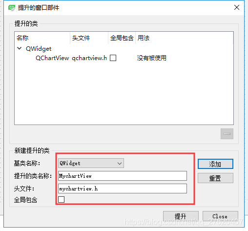
Promote QT default control to custom control
【ACM】455. 分发饼干(1. 大饼干优先喂给大胃口;2. 遍历两个数组可以只用一个for循环(用下标索引--来遍历另一个数组))

Install the yapiupload plug-in in idea and upload the API interface to the Yapi document
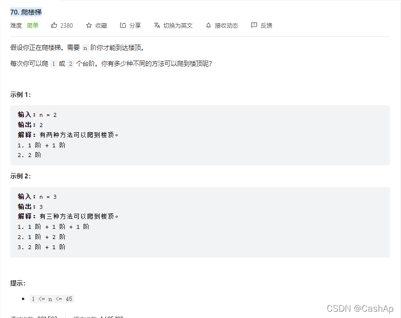
【ACM】70. 爬楼梯
教你用简单几个步骤快速重命名文件夹名
随机推荐
MATLAB从入门到精通(二)
Log4j2 cross thread print traceid
Test post and login function
Kettle paoding jieniu Chapter 17 text file output
Introduction to quantexa CDI syneo platform
Pointers in rust: box, RC, cell, refcell
关于unity文件读取的操作(一)
CANopen STM32 transplantation
STM32学习记录0008——GPIO那些事1
According to the result set queried by SQL statement, it is encapsulated as JSON
Software test summary
ctfshow-web361(SSTI)
RC smart pointer in rust
Resolve the error Max virtual memory areas VM max_ map_ count [65530] is too low, increase to at least [262144]
Gst-launch-1.0 usage notes
How to restore MySQL database after win10 system is reinstalled (mysql-8.0.26-winx64. Zip)
Can filter
Custom prompt box MessageBox in QT
根据快递单号查询物流查询更新量
Daily network security certification test questions (April 12, 2022)