当前位置:网站首页>FPGA - Memory Resources of 7 Series FPGA Internal Structure -03- Built-in Error Correction Function
FPGA - Memory Resources of 7 Series FPGA Internal Structure -03- Built-in Error Correction Function
2022-08-10 22:01:00 【Vuko-wxh】
Summary of built-in error correction
使用 72 位宽 RAM 中的额外 8 位,Simple two-port mode RAMB36E1 Can be configured to have built-in hamming code error correction function of single 512 x 64 RAM. 该操作是透明的.
At any one time during the write operation will generate eight protection a (ECCPARITY),并与 64 A data store into the memory together. 这些 ECCPARITY In each read during operation is used to correct any mistakes,或检测(但不纠正)Any two position error.ECCPARITY 位在 WRCLK Each rise along are written to the memory and output to the FPGA 逻辑. ECCPARITY There is no available optional output bit output register.
At any one time during read operations,从存储器中读取 72 位数据(64 位数据和 8 位奇偶校验位)并馈送到 ECC 解码器. ECC Decoder generates two state output(SBITERR 和 DBITERR),Used to indicate three possible to read the results:无错误、Unit has been rectified mistakes、Two position error detected. 在标准 ECC 模式下,Read operation will not correct the mistakes in memory array,它只会在 DO Corrected data on. 为了提高 FMAX,由 DO_REG Attributes control the optional register can be used for data output (DO)、SBITERR 和 DBITERR.
ECC Configuration options can be used for simple two-port mode 36Kb 块 RAM (RAMB36E1) 或 36Kb FIFO (FIFO36E1). RAMB36E1 Have the ability to inject errors. RAMB36E1 Able to read the data back to read the current address. This function to better support to repair a mistake or invalidate the contents of the address for future visit. FIFO36E1 支持标准 ECC And the pattern error injection and. FIFO36E1 不支持 ECC Coding mode and not only the output is being read address location.
7 系列 FPGA 块 RAM ECC 还支持 READ_FIRST 和 WRITE_FIRST 模式,其方式与 SDP 模式相同.
ECC 模式
在标准 ECC 模式(EN_ECC_READ = TRUE 和 EN_ECC_WRITE = TRUE)中,The encoder and decoder are enabled. 在写入期间,64 位数据和 8 位 ECC The generated parity is stored in the array. External parity bits are ignored. 在读取过程中,72 A decoding data and parity was read out.
The encoder and the decoder can separate in simple two-port mode access for external use RAMB36E1. Used alone encoder,需要通过DI口发送数据,ECCPARITYOutlet can sampling. To use decoder alone,禁用编码器,将数据写入 Block RAM,并从 Block RAM Read the correct data and status of.
要在 ECC Only USES decoder decoding mode,请设置 EN_ECC_WRITE = FALSE 和 EN_ECC_READ = TRUE.
There are two kinds of encoder use:
- 要在标准 ECC Mode using the encoder,请设置 (EN_ECC_WRITE = TRUE 和 EN_ECC_READ = TRUE). 在这种模式下,不支持 ECC 奇偶校验.
- To use only the encoder mode,请设置(EN_ECC_WRITE = TRUE 和 EN_ECC_READ = FALSE). 在这种模式下,支持 ECC 奇偶校验.
使用 ECC 模式时 Block RAM 的功能描述如下:
- Block RAM Port still have separate address、The clock and can make the input,But a port is a special writing port,The other is a special read port( 简单的双端口).
- DO Said after the correction of reading data.
- DO 保持有效,Until the next effective read operations.
- To allow for different reading at the same time/Write the address decoding and encoding; 但是,Don't allow to read the same at the same time/Write the address decoding and encoding.
- 在ECC 配置中,块RAM 可以处于READ_FIRST 或WRITE_FIRST 模式.
Block RAM ECC 架构的顶层视图
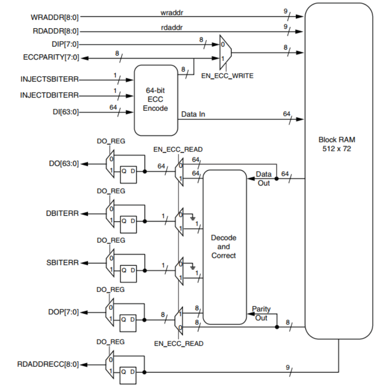
Block RAM 和 FIFO ECC 原语
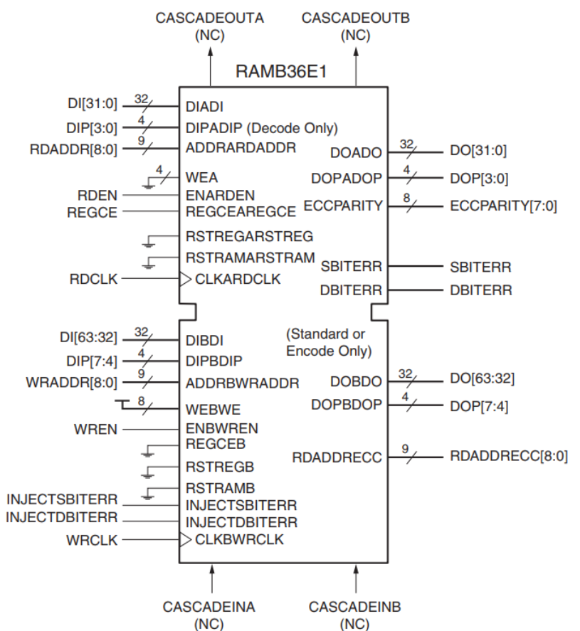
下图显示了 Block RAM (RAMB36E1) ECC 原语. Only simple dual port (SDP) 模式下的 RAMB36E1 支持 ECC.
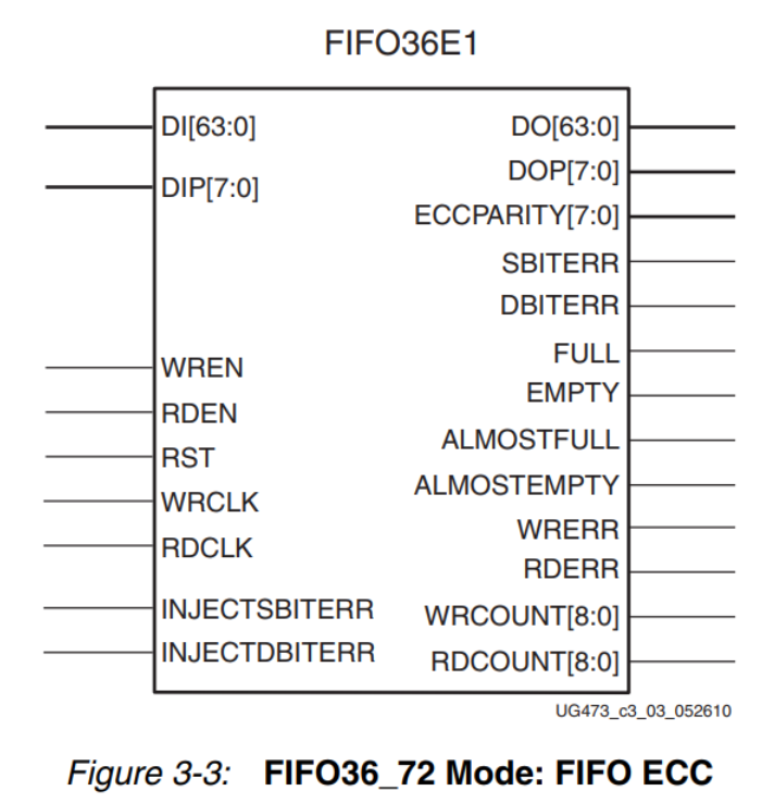
下图显示了 FIFO36E1 ECC 原语. FIFO36_72 Only supports the standard ECC 模式,不支持 RDADDRECC 输出.
Block RAM 和 FIFO ECC 端口说明
The following table lists and describes Block RAM ECC I/O 端口名称.
| Port Name | Signal Description |
|---|---|
| DIADI[31:0] | 在 ECC 模式下由 ADDRBWRADDR 寻址的端口 A 数据输入. |
| DIPADIP[3:0] | 在 ECC 模式下由 ADDRBWRADDR 寻址的端口 A 数据奇偶校验输入. |
| DIBDI[31:0] | 由 ADDRBWRADDR 寻址的端口 B 数据输入. |
| DIPBDIP[3:0] | 由 ADDRBWRADDR 寻址的端口 B 数据奇偶校验输入. |
| ADDRARDADDR [15:0] | 端口 A 地址输入总线. 在 RAM_MODE = SDP 中,这是 RDADDR 总线. 在 ECC 模式下,Use only a [14:6]. |
| ADDRBWRADDR[15:0] | 端口 B 地址输入总线. 在 RAM_MODE = SDP 中,这是 WRADDR 总线. 在 ECC 模式下,Use only a [14:6]. |
| WEA[3:0] | 端口 A 字节宽的写使能. 在 RAM_MODE = SDP 中不使用. 在 ECC 模式下,将 WEA 连接到 GND. |
| WEBWE[7:0] | 端口 B 字节宽写使能 (WEBWE [3:0]). 在 RAM_MODE = SDP 中,这是字节范围的写使能. 在 ECC 模式下,Connect the port to logic high level. |
| ENARDEN | 端口 A 启用. 在 RAM_MODE = SDP 或 ECC 中,这是 RDEN. |
| ENBWREN | 端口 B 启用. 在 RAM_MODE = SDP 或 ECC 中,这是 WREN. |
| RSTREGARSTREG | 同步输出寄存器设置/复位由 SRVAL_A (DO_REG = 1) 初始化. RSTREG_PRIORITY_A 确定 REGCE 的优先级. 在 RAM_MODE = SDP 中,这是 RSTREG. 在 ECC 模式下,将RSTREGARSTREG 连接到GND. |
| RSTREGB | 同步输出寄存器设置/复位由 SRVAL_B (DO_REG = 1) 初始化. RSTREG_PRIORITY_B 确定 REGCE 的优先级. 在 SDP (ECC) 模式下,将 RSREGB 连接到 GND. |
| RSTRAMARSTRAM | 同步输出锁存器设置/复位由 SRVAL_A (DO_REG = 0) 初始化. 在 RAM_MODE = SDP 中,这是 RSTRAM. 在 ECC 模式下,连接到 GND. |
| RSTRAMB | 同步输出锁存器设置/复位由 SRVAL_B (DO_REG = 0) 初始化. 在 SDP (ECC) 模式下,将 REGCEB 连接到 GND. |
| CLKARDCLK | 端口 A 时钟输入. 在 RAM_MODE = SDP 中,这是 RDCLK. |
| CLKBWRCLK | 端口 B 时钟输入. 在 RAM_MODE = SDP 中,这是 WRCLK. |
| REGCEAREGCE | 端口 A 输出寄存器时钟使能 (DO_REG = 1). 在 RAM_MODE SDP 和 ECC 中,这是 REGCE. |
| REGCEB | 端口 B 输出寄存器时钟使能 (DO_REG = 1). 在 ECC 模式下,将 REGCEB 连接到 GND. |
| CASCADEINA | 端口 A 级联输入. 仅用于 RAM_MODE = TDP. |
| CASCADEINB | 端口 B 级联输入. 仅用于 RAM_MODE = TDP. |
| CASCADEOUTA | 端口 A 级联输出. 仅用于 RAM_MODE = TDP. |
| CASCADEOUTB | 端口 B 级联输出. 仅用于 RAM_MODE = TDP. |
| DOADO[31:0] | 由 ADDRARDADDR 寻址的端口 A 数据输出总线. |
| DOPADOP[3:0] | 由 ADDRARDADDR 寻址的端口 A 奇偶校验输出总线. |
| DOBDO[31:0] | 端口 B 由 ADDRARDADDR Addressing the data output of the bus. |
| DOPBDOP[3:0] | 端口 B 奇偶校验输出总线由 ADDRARDADDR 寻址. |
| ECC Port Names (Not used if RAM_MODE = TDP) | |
| INJECTSBERR | 如果使用 ECC,The injection unit error. During the period of writing when setting,在特定的 Block RAM Position error creating unit. To read the position,Block RAM ECC Logic will correct this error. Error in office DI[30] 中产生. |
| INJECTDBERR | 如果使用 ECC,Is injected into two position error. During the period of writing when setting,In two specific Block RAM Position error creating two position. To read the position,Block RAM ECC Logic will mark a two position error. 当 INJECTSBERR 和 INJECTDBERR Signal setting at the same time,Will be injected into two position error. Error in office DI[30] 和 DI[62] 中产生. |
| ECCPARITY[7:0] | ECC 编码器输出总线,Used for coding mode use only ECC. |
| SBITERR | ECC Unit error output state. |
| DBITERR | ECC Two position error output state. |
| RDADDRECC[8:0] | ECC 读取地址. Pointer to the current address of data read. Available data and the corresponding address in the same cycle. |
FIFO ECC 端口名称和说明
| Port Name | Direction | Signal Description |
|---|---|---|
| DI[63:0] | Input | 数据输入总线 |
| DIP[7:0] | Input | 数据输入奇偶校验总线. When using the standard model does not use. |
| WREN | Input | 写使能. 当 WREN = 1 时,数据写入内存. 当 WREN = 0 时,禁止写入. |
| RDEN | Input | 读使能. 当 RDEN = 1 时,从内存中读取数据. 当 RDEN = 0 时,读取被禁用. |
| RSTREG | Input | 使用 Block RAM ECC When primitive does not support. Always connected to GND. |
| RSTRAM | Input | 使用 Block RAM ECC When primitive does not support. Always connected to GND. |
| RST | Input | FIFO Counter and marking of the asynchronous reset. Must be in three clock cycle assertion reset. Reset does not affect the DO 或 ECC 信号. |
| WRCLK | Input | Write the clock. |
| RDCLK | Input | Read the clock. |
| INJECTSBITERR | Input | During the period of writing when setting,在特定的 Block RAM Generating unit in a mistake. To read the position,Block RAM ECC Logic will correct this error. Error in office DI[30] 中产生. |
| INJECTDBITERR | Input | During the period of writing when setting,In two specific Block RAM A two position error on the. To read the position,Block RAM ECC Logic will mark a two position error. 当两个 INJECTBITERR Signal setting at the same time,Will be injected into a two position error. Error in office DI[30] 和 DI[62] 中产生. |
| DO[63:0] | Output | 数据输出总线 |
| DOP[7:0] | Output | 数据输出奇偶校验总线. |
| SBITERR | Output | 单位错误状态. |
| DBITERR | Output | 双位错误状态. |
| ECCPARITY[7:0] | Output | 不支持. |
| FULL | Output | FIFO 满标志. |
| ALMOSTFULL | Output | FIFO Almost the full mark. |
| EMPTY | Output | FIFO 空标志. |
| ALMOSTEMPTY | Output | FIFO Almost empty sign. |
| RDCOUNT | Output | FIFO 数据读取指针. |
| WRCOUNT | Output | FIFO 数据写指针. |
| WRERR | Output | 当 FIFO 已满时,任何额外的写操作都会生成一个错误标志. |
| RDERR | Output | 当 FIFO 为空时,任何额外的读取操作都会生成错误标志. |
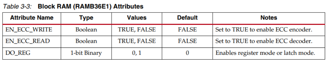
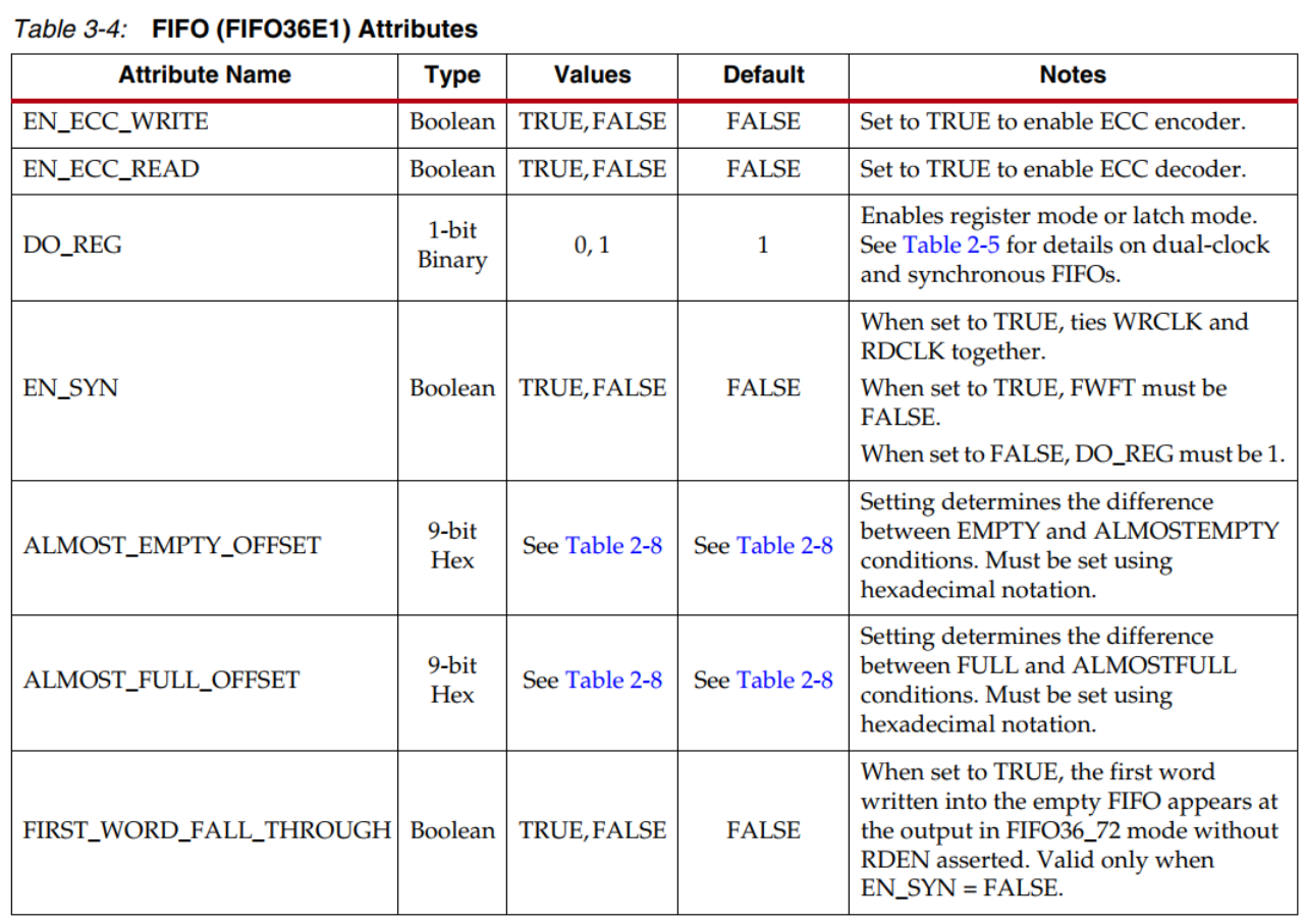
Block RAM 和 FIFO ECC 属性
In addition to decoding and correct the built-in registers in logic,RAMB36E1 Primitive allows you to use by DO_REG Attributes control the optional pipeline register,To produce a higher performance and an additional delay. 下表列出了 Block RAM 和 FIFO ECC 属性.
ECC 操作模式
ECC Operation is divided into three types:标准、Only the encoding and decoding only. 标准 ECC Model at the same time using the encoder and decoder.
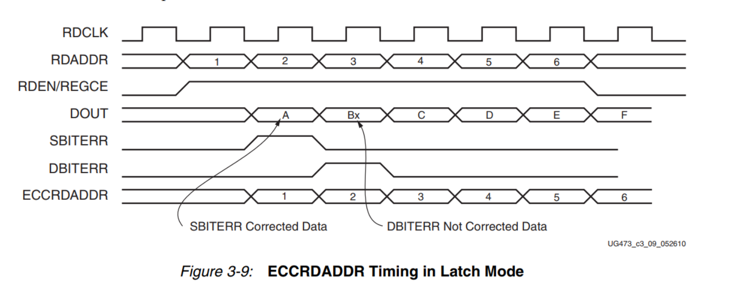
图 3-4 到图 3-9 显示了 Block RAM 和 FIFO 中 ECC Several kinds of operating modes. 由用户提供 Block RAM WRADDR 和 RDADDR 地址输入.FIFO WRADDR 和 RDADDR Address is generated internally by write counter and read on.
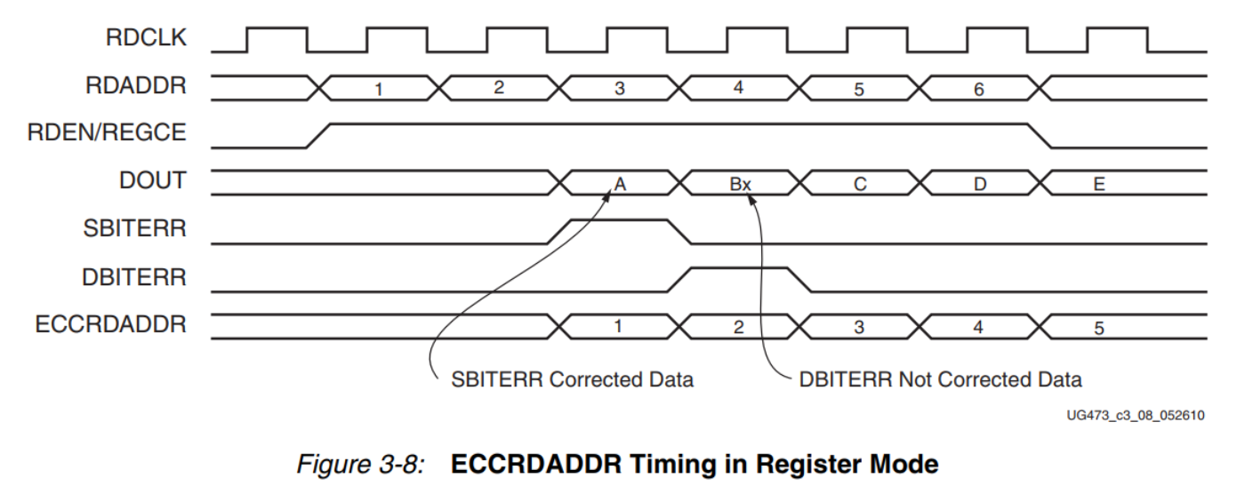 数据(DOUT)And the corresponding address(ECCRDADDR)Used in the same phase provide.
数据 (DOUT) And the corresponding address (ECCRDADDR) Used in the same phase provide.
标准ECC
By the property SettingsECC
E N _ E C C _ R E A D = T R U E E N _ E C C _ W R I T E = T R U E EN\_ECC\_READ = TRUE\\ EN\_ECC\_WRITE = TRUE EN_ECC_READ=TRUEEN_ECC_WRITE=TRUE
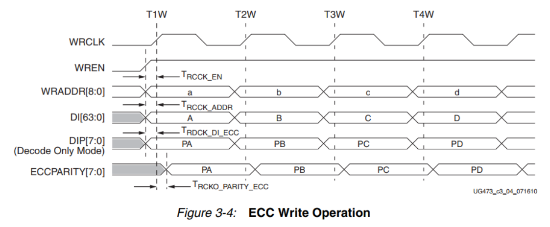
标准 ECC 写入
如图 3-4 所示.
在时间 T1W,DI[63:0] = A Are written to the memory location a. Generated inside the corresponding 8 位 ECC 奇偶校验 PA(十六进制),附加到 64 个数据位后,写入内存. 写入后,奇偶校验值 PA Immediately appear in the output ECCPARITY[7:0]. 因为 ECC Parity is internally generated,所以不使用 DIP[7:0] 引脚. 在标准 ECC 模式下,不支持 ECC 奇偶校验.
类似地,在时间 T2W 和 T3W,DI[63:0] = B 和 C,Along with their corresponding parity bit PB(十六进制)和 PC(十六进制)Are written to the storage unit b 和 c. PB 和 PC 在 T2W 和 T3W Shortly after the appear in the output ECCPARITY[7:0].
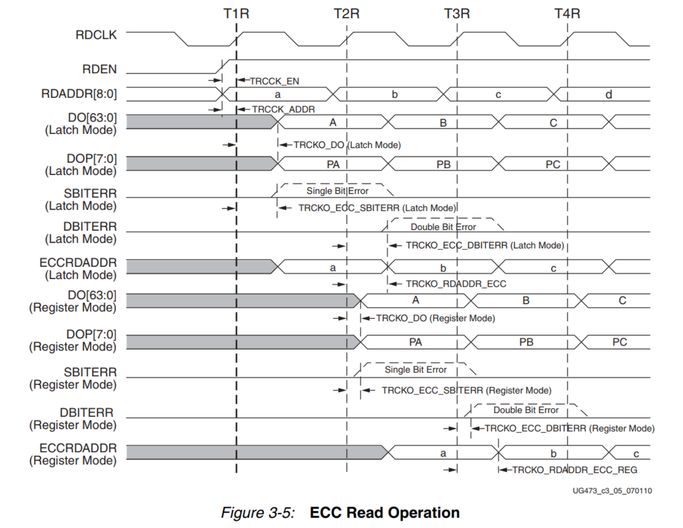
标准 ECC 读取
如图 3-5 所示.
在时间 T1R,Read internal address location a 的 72 A memory content,包括 64 位数据 A 和 8 位奇偶校验 PA(十六进制). 如果没有错误,则在 DO[63:0] 和 DOP[7:0] Output the original data and parity check. If the data or units exist in the parity error,The correct mistakes,并且 SBITERR 为高. If the data and parity exist two position error,The error is not correct. Output the original data and parity check,DBITERR 为高.如果属性 DO_REG 设置为 0,则在 T1R 之后不久,DO[63:0] = A 和 DOP[7:0] = PA.
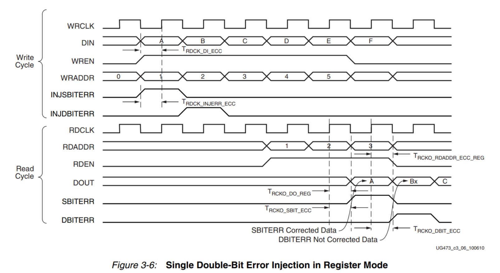
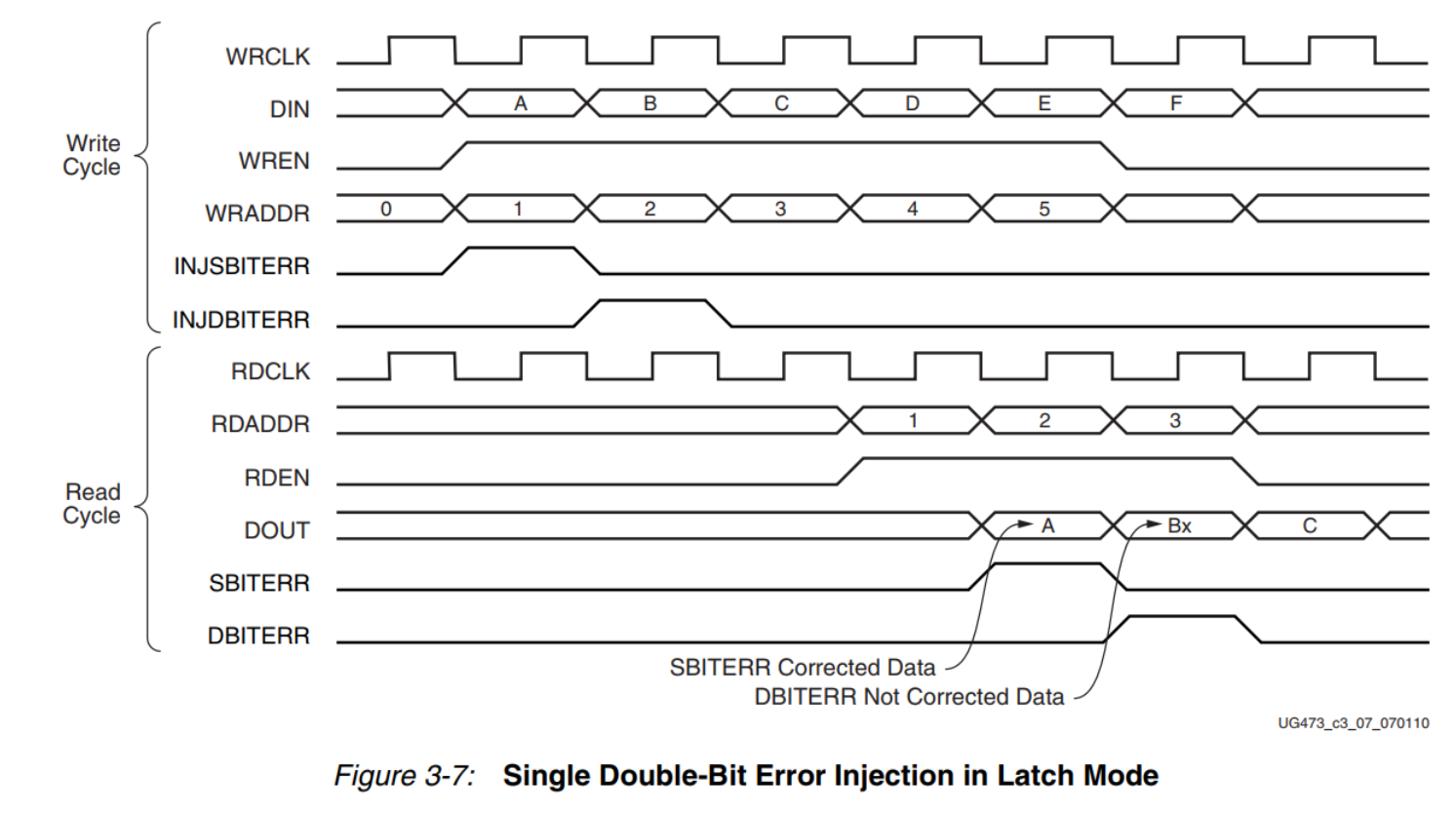
类似地,在时间 T2R 和 T3R,地址位置 b 和 c The memory contents in DO[63:0] 和 DOP[7:0] By reading and decoding. If the data set A Detected on the unit or two position error,SBITERR/DBITERR The output is also available in T1R 之后切换.图 3-7 Shows in the clock T1R 和 在时钟沿 T2R 之后,The latch mode in data B Two position error is detected on the (DBITERR).
如果属性 DO_REG 设置为 1,则在 T2R 之后不久,DO[63:0] = A 和 DOP[7:0] = PA.
类似地,在时间 T3R 和 T4R,地址位置 b 和 c The memory contents in DO[63:0] 和 DOP[7:0] By reading and decoding. If the data set A On a single bit or bit error detected,SBITERR/DBITERR The output is also available in T2R 之后切换.图 3-6 Display in the clock T2R 和 在时钟沿 T3R 之后,In the register mode detected data B The two position on the error (DBITERR).
仅 ECC 编码
By the property Settings
E N _ E C C _ R E A D = F A L S E E N _ E C C _ W R I T E = T R U E EN\_ECC\_READ = FALSE\\ EN\_ECC\_WRITE = TRUE EN_ECC_READ=FALSEEN_ECC_WRITE=TRUE
ECC Only code written to
在时间 T1W,DI[63:0] = A Are written to the memory location a. Generated inside the corresponding 8 位 ECC 奇偶校验 PA(十六进制),附加到 64 个数据位后,写入内存. 写入后,奇偶校验值 PA Immediately appear in the output ECCPARITY[7:0]. 因为 ECC Parity is internally generated,所以不使用 DIP[7:0] 引脚.
类似地,在时间 T2W 和 T3W,DI[63:0] = B 和 C,Along with their corresponding parity bit PB(十六进制)和 PC(十六进制)Are written to the storage unit b 和 c. PB 和 PC 在 T2W 和 T3W Shortly after the appear in the output ECCPARITY[7:0].
ECC Only code read
ECC Code read only with ordinary piece of RAM 读取相同. 64 A data appeared in the DO[63:0],8 A parity check in DOP[7:0]. Won't unit error correction,And error sign SBITERR 和 DBITERR Was never assert that.
仅 ECC 解码
By the property Settings
E N _ E C C _ R E A D = T R U E E N _ E C C _ W R I T E = F A L S E EN\_ECC\_READ = TRUE\\EN\_ECC\_WRITE = FALSE EN_ECC_READ=TRUEEN_ECC_WRITE=FALSE
在 ECC Only in the decoding,仅启用 ECC 解码器. ECC The encoder is disabled.Only decoding mode used for injection unit or two position error to test ECC The function of the decoder. ECC Parity bit must be used DIP[7:0] Pin from the outside to provide.
仅使用 ECC Decoding to injection unit error
- 在时间 T1W、T2W、T3W、DI[63:0] = A、B、C Unit of mistakes, and DIP[7:0] = PA(十六进制)、PB (hex)、PC (hex),将 A、B 和 C 的相应 ECC Parity bit write memory location a、b 和 c.
- 在时间T1R、T2R、T3R,地址a、b和cContent has been read and according to the need for correction.
- 锁存模式:DO[63:0] = A, B, C, DOP[7:0] = PA, PB, PC 在 T1R、T2R、T3R 之后不久.
- 寄存器模式:DO[63:0] = A, B, C, DOP[7:0] = PA, PB, PC 在 T2R、T3R、T4R 之后不久.
- SBITERR 与相应的 DO/DOP 数据对齐.
ECC Units in the decoder is also correct the parity bit error
- 在时间 T1W、T2W、T3W、DI[63:0] = A、B、C A double error and DIP[7:0] = PA(十六进制)、PB(十六进制)、PB(十六进制)时, A、B 和 C 的相应 ECC Parity bit is written to memory location a、b 和 c.
- 在时间T1R、T2R、T3R,地址a、b、c The original content of the error has been detected by the readout and two position.
- 锁存模式:DO[63:0] = A、B、C There are two position error,DOP[7:0] = PA、PB、PC 在 T1R、T2R、T3R 之后不久.
- 寄存器模式:DO[63:0] = A, B, C There are two position error,DOP[7:0] = PA, PB, PC 在 T2R, T3R, T4R 之后不久.
- DBITERR 与相应的 DO/DOP 数据对齐.
ECCDecoder also detect parity bit when two position error,And data when unit errors, and the corresponding parity bit unit error when.
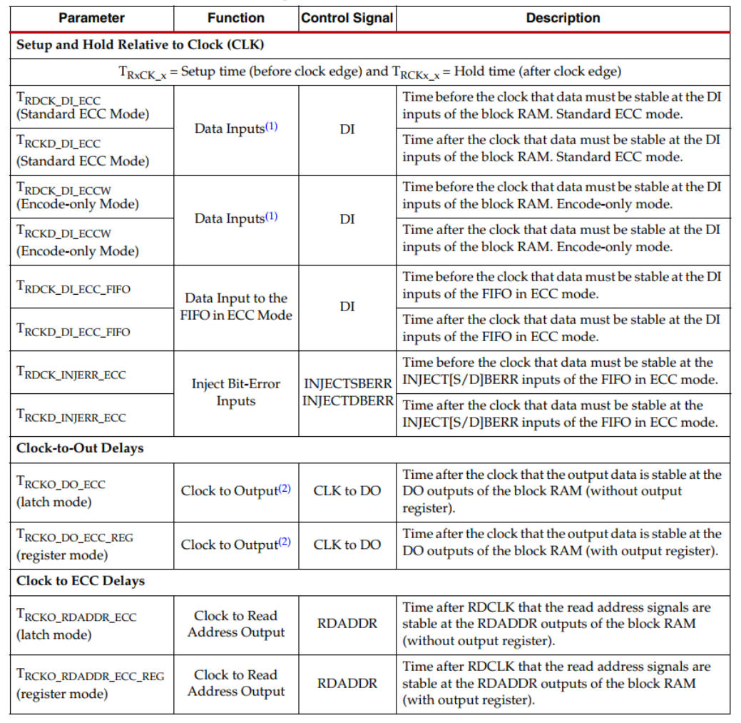
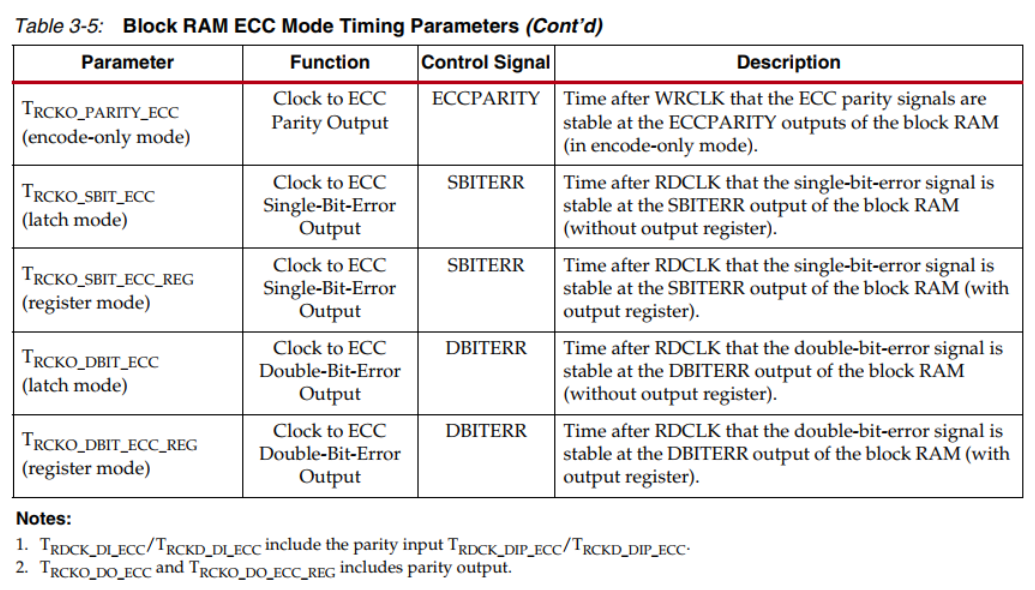
ECC 时序特性
图 3-4 至图 3-7 Also shows the various ECC 时序参数.Because the write clock and read clocks are independent of each other,所以图 3-4 The end of all write timing is a WRCLK 为参考. 图 3-5 All read in sequence to RDCLK 为参考.
标准 ECC 写时序
参见图 3-4.
- 在时间TRCCK_EN,在时间T1W 之前,写使能在Block RAM 的WREN 输入处变为有效.
- 在时间T1W 之前的TRCCK_ADDR 时间,写入地址a 在块RAM 的WRADDR[8:0] 输入处变为有效. FIFO 不需要 WRADDR 输入.
- 在时间TRDCK_DI_ECC(标准ECC),在时间T1W 之前,写入数据A(十六进制)在块RAM 的DI[63:0] 输入处变为有效.
- 在时间TRCKO_ECC_PARITY(标准ECC),在时间T1W 之后,ECC 奇偶校验数据PA(十六进制)在块RAM 的ECCPARITY[7:0] Output pin place into effective.
标准 ECC 读时序
请参见图 3-5.
- 在时间TRCCK_EN,在时间T1R 之前,Reading can make the blockRAM 的RDEN 输入处变为有效.
- 在时间TRCCK_ADDR,在时间T1R 之前,写入地址a 在块RAM 的RDADDR[8:0] 输入处变为有效. FIFO 不需要 RDADDR 输入.
DO_REG = 0
- 在时间TRCKO_DO(锁存模式),时间T1R 之后,数据A(十六进制)在Block RAM 的DO[63:0] 输出引脚上变为有效.
- 在时间 TRCKO_DOP(锁存模式),时间 T1R 之后,数据 PA(十六进制)在 Block RAM 的 DOP[7:0] 输出引脚上变为有效.
- 在时间 TRCKO_ECC_SBITERR(锁存模式),在时间 T1R 之后,If the data set A Detect and correct the single bit error,则 SBITERR 被置位.
- 在时间 TRCKO_ECC_DBITERR(锁存模式),时间 T2R 之后,If the data set B Two position error is detected on the,则断言 DBITERR.
DO_REG = 1
- 在时间TRCKO_DO(寄存器模式),时间T2R 之后,数据A(十六进制)在Block RAM 的DO[63:0] 输出引脚上变为有效.
- 在时间TRCKO_DOP(寄存器模式),时间T2R 之后,数据PA(十六进制)在块RAM 的DOP[7:0] 输出引脚上变为有效.
- 在时间 TRCKO_ECCR_SBITERR(寄存器模式),时间 T2R 之后,If the data set A Detect and correct the single bit error,则断言 SBITERR.
- 在时间 TRCKO_ECCR_DBITERR(寄存器模式),时间 T3R 之后,If the data set B Two position error is detected on the,则断言 DBITERR.
仅编码 ECC 写入时序
请参见图 3-4.
- WREN 和WRADDR 的建立/Keep time with the standardECC 相同.
- 在时间TRDCK_DI_ECC(仅编码ECC),在时间T1W 之前,写入数据A(十六进制)在块RAM 的DI[63:0] 输入处变为有效.
- 在时间TRCKO_ECC_PARITY(仅编码ECC),在时间T1W 之后,ECC 奇偶校验数据PA(十六进制)在Block RAM 的ECCPARITY[7:0] 输出引脚上变为有效.
仅编码 ECC 读取时序
- 仅编码 ECC Read sequence and normal Block RAM Read the sequence the same.
Only the decoding ECC 写入时序
- Only the decoding ECC Write sequence and normal Block RAM Write sequence is the same.
Only the decoding ECC 读取时序
- Only the decoding ECC Read sequence and standard ECC Read the sequence the same.
Block RAM ECC Model parameters
下表显示了 7 系列 FPGA 的 Block RAM ECC Model parameters.
为 64 To create a word 8 个奇偶校验位
使用块 RAM The logic of the external(大量 XOR 电路),可以为 64 To create a word 8 个奇偶校验位. 但是,使用仅 ECC 编码器模式,Any will 64 A word write separate Block RAM 来自动创建 8 个奇偶校验位,而无需额外的逻辑. 编码后的 8 位 ECC Parity data immediately available,Or you can read the full 72 位字.
边栏推荐
猜你喜欢
JVM classic fifty questions, now the interview is stable

PROCEDURE :存储过程结构——《mysql 从入门到内卷再到入土》
Use Cloudreve to build a private cloud disk
Huawei router clock near the drainage experiment (using stream strategy)
Live Classroom System 09--Tencent Cloud VOD Management Module (1)
APP UI自动化测试常见面试题,或许有用呢~
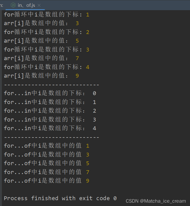
ES6中的for...in/of的使用

翻译科技论文,俄译中怎样效果好
这些不可不知的JVM知识,我都用思维导图整理好了
使用SylixOS虚拟串口,实现系统串口自由
随机推荐
Bedtime story | made a Bitmap and AST length system configuration
UPDATE:修改数据语法使用例——《mysql 从入门到内卷再到入土》
C. Rotation Matching
camera preview process --- from HAL to OEM
ES6中的for...in/of的使用
力扣215题,数组中的第K个最大元素
直播课堂系统08补-腾讯云对象存储和课程分类管理
Huawei router clock near the drainage experiment (using stream strategy)
In 2021 China industrial Internet security competition (competition) in fujian province and the first industry of fujian province Internet innovation competition
ENVI自动生成地面控制点实现栅格影像的自动地理配准
C. Even Picture
LeetCode-498 - Diagonal Traversal
石油化工行业商业供应链管理系统:标准化供应商管理,优化企业供应链采购流程
LeetCode-498-对角线遍历
ACM解题笔记——HDU 1401 Solitaire(DBFS)
为什么一般公司面试结束后会说「回去等消息」,而不是直接告诉面试者结果?
DDL:视图——《mysql 从入门到内卷再到入土》
ACM模板笔记:八数码问题——使用BFS+康托展开打表解决
MATLAB神经网络拟合工具箱Neural Net Fitting使用方法
黑猫带你学Makefile第12篇:常见Makefile问题汇总