当前位置:网站首页>STM32-库函数-SetSysClock(void)函数解析-正点原子探索者
STM32-库函数-SetSysClock(void)函数解析-正点原子探索者
2022-08-11 05:25:00 【Archimedes' boat】
目录
笔记:总代码&时钟结构图
总目的:配置SYSCLK(最高168MHz)
时钟选择源:PLLCLK
函数代码源:USER\system_stm32f4xx.c
static void SetSysClock(void)
{
#if defined (STM32F40_41xxx) || defined (STM32F427_437xx) || defined (STM32F429_439xx) || defined (STM32F401xx)
/******************************************************************************/
/*            PLL (clocked by HSE) used as System clock source                */
/******************************************************************************/
  __IO uint32_t StartUpCounter = 0, HSEStatus = 0;

  /* Enable HSE */
  RCC->CR |= ((uint32_t)RCC_CR_HSEON);

  /* Wait till HSE is ready and if Time out is reached exit */
  do
  {
    HSEStatus = RCC->CR & RCC_CR_HSERDY;
    StartUpCounter++;
  } while((HSEStatus == 0) && (StartUpCounter != HSE_STARTUP_TIMEOUT));

  if ((RCC->CR & RCC_CR_HSERDY) != RESET)
  {
    HSEStatus = (uint32_t)0x01;
  }
  else
  {
    HSEStatus = (uint32_t)0x00;
  }

  if (HSEStatus == (uint32_t)0x01)
  {
    /* Select regulator voltage output Scale 1 mode */
    RCC->APB1ENR |= RCC_APB1ENR_PWREN;
    PWR->CR |= PWR_CR_VOS;

    /* HCLK = SYSCLK / 1*/
    RCC->CFGR |= RCC_CFGR_HPRE_DIV1;

#if defined (STM32F40_41xxx) || defined (STM32F427_437xx) || defined (STM32F429_439xx)
    /* PCLK2 = HCLK / 2*/
    RCC->CFGR |= RCC_CFGR_PPRE2_DIV2;

    /* PCLK1 = HCLK / 4*/
    RCC->CFGR |= RCC_CFGR_PPRE1_DIV4;
#endif /* STM32F40_41xxx || STM32F427_437x || STM32F429_439xx */

#if defined (STM32F401xx)
    /* PCLK2 = HCLK / 2*/
    RCC->CFGR |= RCC_CFGR_PPRE2_DIV1;

    /* PCLK1 = HCLK / 4*/
    RCC->CFGR |= RCC_CFGR_PPRE1_DIV2;
#endif /* STM32F401xx */

    /* Configure the main PLL */
    RCC->PLLCFGR = PLL_M | (PLL_N << 6) | (((PLL_P >> 1) -1) << 16) |
                   (RCC_PLLCFGR_PLLSRC_HSE) | (PLL_Q << 24);

    /* Enable the main PLL */
    RCC->CR |= RCC_CR_PLLON;

    /* Wait till the main PLL is ready */
    while((RCC->CR & RCC_CR_PLLRDY) == 0)

		;

#if defined (STM32F427_437xx) || defined (STM32F429_439xx)
    /* Enable the Over-drive to extend the clock frequency to 180 Mhz */
    PWR->CR |= PWR_CR_ODEN;
    while((PWR->CSR & PWR_CSR_ODRDY) == 0)
    {
    }
    PWR->CR |= PWR_CR_ODSWEN;
    while((PWR->CSR & PWR_CSR_ODSWRDY) == 0)
    {
    }
    /* Configure Flash prefetch, Instruction cache, Data cache and wait state */
    FLASH->ACR = FLASH_ACR_PRFTEN | FLASH_ACR_ICEN |FLASH_ACR_DCEN |FLASH_ACR_LATENCY_5WS;
#endif /* STM32F427_437x || STM32F429_439xx  */

#if defined (STM32F40_41xxx)
    /* Configure Flash prefetch, Instruction cache, Data cache and wait state */
    FLASH->ACR = FLASH_ACR_PRFTEN | FLASH_ACR_ICEN |FLASH_ACR_DCEN |FLASH_ACR_LATENCY_5WS;
#endif /* STM32F40_41xxx  */

#if defined (STM32F401xx)
    /* Configure Flash prefetch, Instruction cache, Data cache and wait state */
    FLASH->ACR = FLASH_ACR_PRFTEN | FLASH_ACR_ICEN |FLASH_ACR_DCEN |FLASH_ACR_LATENCY_2WS;
#endif /* STM32F401xx */

    /* Select the main PLL as system clock source */
    RCC->CFGR &= (uint32_t)((uint32_t)~(RCC_CFGR_SW));
    RCC->CFGR |= RCC_CFGR_SW_PLL;

    /* Wait till the main PLL is used as system clock source */
    while ((RCC->CFGR & (uint32_t)RCC_CFGR_SWS ) != RCC_CFGR_SWS_PLL);
    {
    }
  }
  else
  { /* If HSE fails to start-up, the application will have wrong clock
         configuration. User can add here some code to deal with this error */
  }
}
时钟结构:STM32F4xx中文参考手册.pdf-6.2时钟

看图可知,有五个时钟源,分别为LSE、LSI、HSE、HSI、PLLCLLK
SetSysClock(void)函数就是对时钟源进行初始化,并且设置SYSCLK(系统时钟)
设置过程的代码有一定重复度,清楚模板应该就
------------------------------------------------华-丽-分-割-线------------------------------------------------
段1
首先是前面一段
  __IO uint32_t StartUpCounter = 0, HSEStatus = 0;

  /* Enable HSE */
  RCC->CR |= ((uint32_t)RCC_CR_HSEON);

  /* Wait till HSE is ready and if Time out is reached exit */
  do
  {
    HSEStatus = RCC->CR & RCC_CR_HSERDY;
    StartUpCounter++;
  } while((HSEStatus == 0) && (StartUpCounter != HSE_STARTUP_TIMEOUT));
加上宏定义
#define     __IO    volatile             /*!< Defines 'read / write' permissions */

#define  RCC_CR_HSEON                        ((uint32_t)0x00010000)

#define  RCC_CR_HSERDY                       ((uint32_t)0x00020000)

#if !defined  (HSE_STARTUP_TIMEOUT)
  #define HSE_STARTUP_TIMEOUT    ((uint16_t)0x05000)   /*!< Time out for HSE start up */
#endif /* HSE_STARTUP_TIMEOUT */


typedef unsigned int uint32_t;
首先初始化RCC_CR时钟控制寄存器:RCC->CR |= ((uint32_t)RCC_CR_HSEON);
RCC_CR_HSEON=(uint32_t)0x00010000中“1”是第16位,就是激活(enable,使能)HSE
RCC_CR_HSERDY =((uint32_t)0x00020000)中“1”(二进制)是第17位,HSE刚刚初始化的时候不稳定,当17位是“1”时候才稳定,
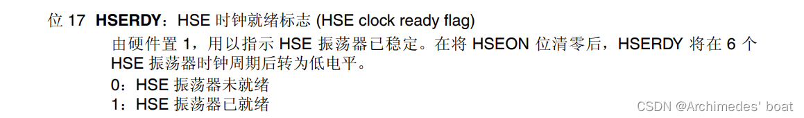
RCC->CR & RCC_CR_HSERDY是说当HSE稳定时候,HSEStatus才不为0,才跳出循环
而StartUpCounter != HSE_STARTUP_TIMEOUT指开始循环计数没有到达规定上限,要是到了规定次数上限,也跳出循环,暂时按下不表
段2
接下来一段
  if ((RCC->CR & RCC_CR_HSERDY) != RESET)
  {
    HSEStatus = (uint32_t)0x01;
  }
  else
  {
    HSEStatus = (uint32_t)0x00;
  }
加上宏定义
typedef enum {RESET = 0, SET = !RESET} FlagStatus, ITStatus;
和上面一样,如果RCC_CR稳定了,就令HSEStatus = (uint32_t)0x01,这说明HSE确实稳定了,然后进入下一阶段
而如果没稳定,赋值0x00,进入段3最后几句的else语句
/*如果HSE启动失败,应用程序将会有错误的时钟
配置。用户可以在这里添加一些代码来处理此错误*/
eg.此时可以判断StartUpCounter的值决定是否要继续enableHSE
段3
最后一部分
  if (HSEStatus == (uint32_t)0x01)
  {
    /* Select regulator voltage output Scale 1 mode */
    RCC->APB1ENR |= RCC_APB1ENR_PWREN;
    PWR->CR |= PWR_CR_VOS;

    /* HCLK = SYSCLK / 1*/
    RCC->CFGR |= RCC_CFGR_HPRE_DIV1;

#if defined (STM32F40_41xxx) || defined (STM32F427_437xx) || defined (STM32F429_439xx)
    /* PCLK2 = HCLK / 2*/
    RCC->CFGR |= RCC_CFGR_PPRE2_DIV2;

    /* PCLK1 = HCLK / 4*/
    RCC->CFGR |= RCC_CFGR_PPRE1_DIV4;
#endif /* STM32F40_41xxx || STM32F427_437x || STM32F429_439xx */

#if defined (STM32F401xx)
    /* PCLK2 = HCLK / 2*/
    RCC->CFGR |= RCC_CFGR_PPRE2_DIV1;

    /* PCLK1 = HCLK / 4*/
    RCC->CFGR |= RCC_CFGR_PPRE1_DIV2;
#endif /* STM32F401xx */

    /* Configure the main PLL */
    RCC->PLLCFGR = PLL_M | (PLL_N << 6) | (((PLL_P >> 1) -1) << 16) |
                   (RCC_PLLCFGR_PLLSRC_HSE) | (PLL_Q << 24);

    /* Enable the main PLL */
    RCC->CR |= RCC_CR_PLLON;

    /* Wait till the main PLL is ready */
    while((RCC->CR & RCC_CR_PLLRDY) == 0)

		;

#if defined (STM32F427_437xx) || defined (STM32F429_439xx)
    /* Enable the Over-drive to extend the clock frequency to 180 Mhz */
    PWR->CR |= PWR_CR_ODEN;
    while((PWR->CSR & PWR_CSR_ODRDY) == 0)
    {
    }
    PWR->CR |= PWR_CR_ODSWEN;
    while((PWR->CSR & PWR_CSR_ODSWRDY) == 0)
    {
    }
    /* Configure Flash prefetch, Instruction cache, Data cache and wait state */
    FLASH->ACR = FLASH_ACR_PRFTEN | FLASH_ACR_ICEN |FLASH_ACR_DCEN |FLASH_ACR_LATENCY_5WS;
#endif /* STM32F427_437x || STM32F429_439xx  */

#if defined (STM32F40_41xxx)
    /* Configure Flash prefetch, Instruction cache, Data cache and wait state */
    FLASH->ACR = FLASH_ACR_PRFTEN | FLASH_ACR_ICEN |FLASH_ACR_DCEN |FLASH_ACR_LATENCY_5WS;
#endif /* STM32F40_41xxx  */

#if defined (STM32F401xx)
    /* Configure Flash prefetch, Instruction cache, Data cache and wait state */
    FLASH->ACR = FLASH_ACR_PRFTEN | FLASH_ACR_ICEN |FLASH_ACR_DCEN |FLASH_ACR_LATENCY_2WS;
#endif /* STM32F401xx */

    /* Select the main PLL as system clock source */
    RCC->CFGR &= (uint32_t)((uint32_t)~(RCC_CFGR_SW));
    RCC->CFGR |= RCC_CFGR_SW_PLL;

    /* Wait till the main PLL is used as system clock source */
    while ((RCC->CFGR & (uint32_t)RCC_CFGR_SWS ) != RCC_CFGR_SWS_PLL);
    {
    }
  }
  else
  { /* If HSE fails to start-up, the application will have wrong clock
         configuration. User can add here some code to deal with this error */
  }
太长了再分段
段3.1
宏定义:
#define  RCC_APB1ENR_PWREN                   ((uint32_t)0x10000000)

#define  PWR_CR_VOS                          ((uint32_t)0x0000C000)     /*!< VOS[1:0] bits (Regulator voltage scaling output selection) */

#define  RCC_CFGR_HPRE_DIV1                  ((uint32_t)0x00000000)        /*!< SYSCLK not divided */
#define  RCC_CFGR_HPRE_DIV2                  ((uint32_t)0x00000080)        /*!< SYSCLK divided by 2 */
#define  RCC_CFGR_HPRE_DIV4                  ((uint32_t)0x00000090)        /*!< SYSCLK divided by 4 */
#define  RCC_CFGR_HPRE_DIV8                  ((uint32_t)0x000000A0)        /*!< SYSCLK divided by 8 */
#define  RCC_CFGR_HPRE_DIV16                 ((uint32_t)0x000000B0)        /*!< SYSCLK divided by 16 */
#define  RCC_CFGR_HPRE_DIV64                 ((uint32_t)0x000000C0)        /*!< SYSCLK divided by 64 */
#define  RCC_CFGR_HPRE_DIV128                ((uint32_t)0x000000D0)        /*!< SYSCLK divided by 128 */
#define  RCC_CFGR_HPRE_DIV256                ((uint32_t)0x000000E0)        /*!< SYSCLK divided by 256 */
#define  RCC_CFGR_HPRE_DIV512                ((uint32_t)0x000000F0)        /*!< SYSCLK divided by 512 */

#define  RCC_CFGR_PPRE1_DIV1                 ((uint32_t)0x00000000)        /*!< HCLK not divided */
#define  RCC_CFGR_PPRE1_DIV2                 ((uint32_t)0x00001000)        /*!< HCLK divided by 2 */
#define  RCC_CFGR_PPRE1_DIV4                 ((uint32_t)0x00001400)        /*!< HCLK divided by 4 */
#define  RCC_CFGR_PPRE1_DIV8                 ((uint32_t)0x00001800)        /*!< HCLK divided by 8 */
#define  RCC_CFGR_PPRE1_DIV16                ((uint32_t)0x00001C00)        /*!< HCLK divided by 16 */


#define  RCC_CFGR_PPRE2_DIV1                 ((uint32_t)0x00000000)        /*!< HCLK not divided */
#define  RCC_CFGR_PPRE2_DIV2                 ((uint32_t)0x00008000)        /*!< HCLK divided by 2 */
#define  RCC_CFGR_PPRE2_DIV4                 ((uint32_t)0x0000A000)        /*!< HCLK divided by 4 */
#define  RCC_CFGR_PPRE2_DIV8                 ((uint32_t)0x0000C000)        /*!< HCLK divided by 8 */
#define  RCC_CFGR_PPRE2_DIV16                ((uint32_t)0x0000E000)        /*!< HCLK divided by 16 */

#if defined (STM32F40_41xxx) || defined (STM32F427_437xx) || defined (STM32F429_439xx) || defined (STM32F401xx)
/* PLL_VCO = (HSE_VALUE or HSI_VALUE / PLL_M) * PLL_N */
#define PLL_M      8
#else /* STM32F411xE */
#if defined (USE_HSE_BYPASS)
#define PLL_M      8
#else /* STM32F411xE */
#define PLL_M      16
#endif /* USE_HSE_BYPASS */
#endif /* STM32F40_41xxx || STM32F427_437xx || STM32F429_439xx || STM32F401xx */

/* USB OTG FS, SDIO and RNG Clock =  PLL_VCO / PLLQ */
#define PLL_Q      7

#if defined (STM32F40_41xxx)
#define PLL_N      336
/* SYSCLK = PLL_VCO / PLL_P */
#define PLL_P      2
#endif /* STM32F40_41xxx */


#define  RCC_CR_PLLON                        ((uint32_t)0x01000000)
#define  RCC_CR_PLLRDY                       ((uint32_t)0x02000000)
代码:
    /* Select regulator voltage output Scale 1 mode */
    RCC->APB1ENR |= RCC_APB1ENR_PWREN;
    PWR->CR |= PWR_CR_VOS;

    /* HCLK = SYSCLK / 1*/
    RCC->CFGR |= RCC_CFGR_HPRE_DIV1;

#if defined (STM32F40_41xxx) || defined (STM32F427_437xx) || defined (STM32F429_439xx)
    /* PCLK2 = HCLK / 2*/
    RCC->CFGR |= RCC_CFGR_PPRE2_DIV2;

    /* PCLK1 = HCLK / 4*/
    RCC->CFGR |= RCC_CFGR_PPRE1_DIV4;
#endif /* STM32F40_41xxx || STM32F427_437x || STM32F429_439xx */

#if defined (STM32F401xx)
    /* PCLK2 = HCLK / 2*/
    RCC->CFGR |= RCC_CFGR_PPRE2_DIV1;

    /* PCLK1 = HCLK / 4*/
    RCC->CFGR |= RCC_CFGR_PPRE1_DIV2;
#endif /* STM32F401xx */

    /* Configure the main PLL */
    RCC->PLLCFGR = PLL_M | (PLL_N << 6) | (((PLL_P >> 1) -1) << 16) |
                   (RCC_PLLCFGR_PLLSRC_HSE) | (PLL_Q << 24);

    /* Enable the main PLL */
    RCC->CR |= RCC_CR_PLLON;

    /* Wait till the main PLL is ready */
    while((RCC->CR & RCC_CR_PLLRDY) == 0)

		;
APB1外设时钟enable寄存器(RCC_APB1ENR) 低速APB使能
APB2外设时钟enable寄存器(RCC_APB2ENR) 高速APB使能
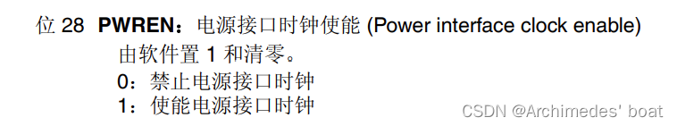
可知RCC_APB1ENR_PWREN=((uint32_t)0x10000000)即为第28位 置1
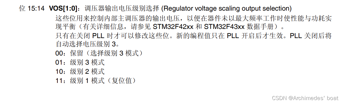
而PWR_CR_VOS=((uint32_t)0x0000C000)即为第14、15位 置1
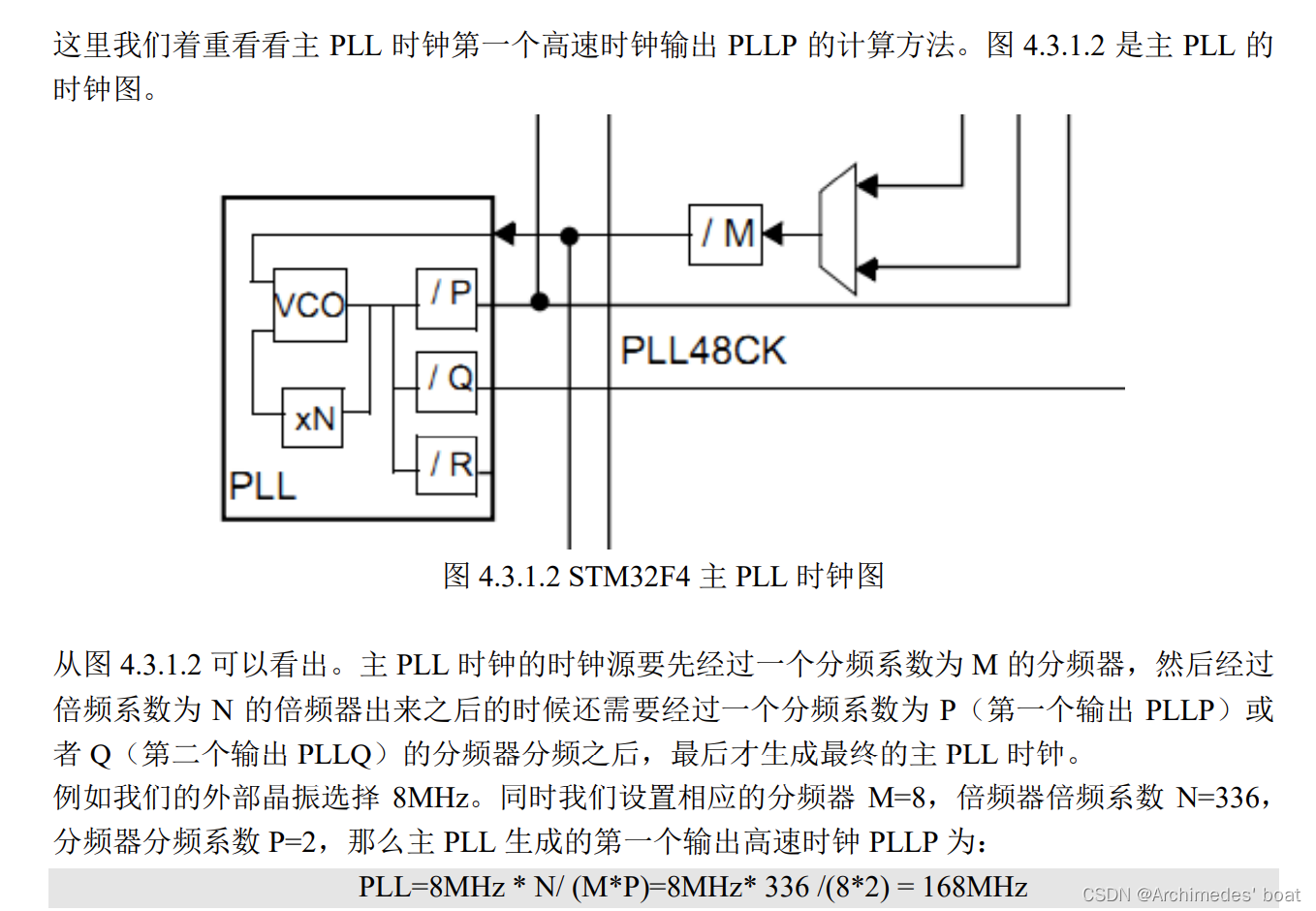
接下来是差分,即时钟结构图上/M,/P,*N等的设置,和上面一样,根据宏定义的数值去查STM32F4xx中文(或英文)参考手册即可找出对应的具体含义
根据差分后的倍率计算公式:
段3.2
#if defined (STM32F427_437xx) || defined (STM32F429_439xx)
    /* Enable the Over-drive to extend the clock frequency to 180 Mhz */
    PWR->CR |= PWR_CR_ODEN;
    while((PWR->CSR & PWR_CSR_ODRDY) == 0)
    {
    }
    PWR->CR |= PWR_CR_ODSWEN;
    while((PWR->CSR & PWR_CSR_ODSWRDY) == 0)
    {
    }
    /* Configure Flash prefetch, Instruction cache, Data cache and wait state */
    FLASH->ACR = FLASH_ACR_PRFTEN | FLASH_ACR_ICEN |FLASH_ACR_DCEN |FLASH_ACR_LATENCY_5WS;
#endif /* STM32F427_437x || STM32F429_439xx  */

#if defined (STM32F40_41xxx)
    /* Configure Flash prefetch, Instruction cache, Data cache and wait state */
    FLASH->ACR = FLASH_ACR_PRFTEN | FLASH_ACR_ICEN |FLASH_ACR_DCEN |FLASH_ACR_LATENCY_5WS;
#endif /* STM32F40_41xxx  */

#if defined (STM32F401xx)
    /* Configure Flash prefetch, Instruction cache, Data cache and wait state */
    FLASH->ACR = FLASH_ACR_PRFTEN | FLASH_ACR_ICEN |FLASH_ACR_DCEN |FLASH_ACR_LATENCY_2WS;
#endif /* STM32F401xx */

    /* Select the main PLL as system clock source */
    RCC->CFGR &= (uint32_t)((uint32_t)~(RCC_CFGR_SW));
    RCC->CFGR |= RCC_CFGR_SW_PLL;

    /* Wait till the main PLL is used as system clock source */
    while ((RCC->CFGR & (uint32_t)RCC_CFGR_SWS ) != RCC_CFGR_SWS_PLL);
    {
    }
  }
  else
  { /* If HSE fails to start-up, the application will have wrong clock
         configuration. User can add here some code to deal with this error */
  }
加上宏定义:
#define  PWR_CR_ODEN                         ((uint32_t)0x00010000)     /*!< Over Drive enable*/
#define  PWR_CR_ODSWEN                       ((uint32_t)0x00020000)     /*!< Over Drive switch enabled */

#define  PWR_CSR_ODRDY                       ((uint32_t)0x00010000)     /*!< Over Drive generator ready */
#define  PWR_CSR_ODSWRDY                     ((uint32_t)0x00020000)     /*!< Over Drive Switch ready */

#define FLASH_ACR_PRFTEN                     ((uint32_t)0x00000100)
#define FLASH_ACR_ICEN                       ((uint32_t)0x00000200)
#define FLASH_ACR_DCEN                       ((uint32_t)0x00000400)

#define FLASH_ACR_LATENCY_2WS                ((uint32_t)0x00000002)
#define FLASH_ACR_LATENCY_5WS                ((uint32_t)0x00000005)

#define  RCC_CFGR_SW                         ((uint32_t)0x00000003)        /*!< SW[1:0] bits (System clock Switch) */
#define  RCC_CFGR_SW_PLL                     ((uint32_t)0x00000002)        /*!< PLL selected as system clock */
#define  RCC_CFGR_SWS                        ((uint32_t)0x0000000C)        /*!< SWS[1:0] bits (System Clock Switch Status) */
Flash 访问控制寄存器 (FLASH_ACR:Flash access control register):Flash 访问控制寄存器用于使能/关闭加速功能,并且可根据 CPU 频率控制 Flash 访问时间,代码上面一段是配置FLASH_ACR来
而RCC->CFGR &= (uint32_t)((uint32_t)~(RCC_CFGR_SW))中:
~(RCC_CFGR_SW)=0x1111111C,又加上&=,最后是除了第0、1位是0,其他位不变,作用是先清零位1:0,再写入PLL,并不是要选择HSI作为系统时钟
紧接着RCC->CFGR |= RCC_CFGR_SW_PLL的作用是选择PLLCLK作为系统时钟
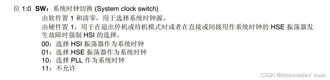
最后的while循环意思是再次确定已经选择了PLLCLK作为系统时钟源
至此系统时钟源设置完毕
总结
1、enable HSE,正点原子的外接HSE是8MHz;
2、把AHB PRESC中APBx分频系数以及其他项设置好;
3、把HSE作为主PLL时钟源;
4、把/M、*N、/P设置好,enable PLLCLK,让PLLCLK就绪;
5、让SYSCLK选择PLLCLK作为时钟源。
边栏推荐
猜你喜欢
智慧工地 安全帽识别系统
Hard hat identification
LiDAR Snowfall Simulation for Robust 3D Object Detection
aPaaS和iPaaS的区别
基于AI智能图像识别:4个不同的行业应用
2022年最新安全帽佩戴识别系统
mAPH——Waymo数据集
TAMNet:A loss-balanced multi-task model for simultaneous detection and segmentation

Use regex to verify whether the file name is legal

Pay “Attention” to Adverse Weather
随机推荐
CNN-based Point Cloud De-Noising
Zhejiang University School of Software 2020 Guarantee Research Computer Real Question Practice
TAMNet:A loss-balanced multi-task model for simultaneous detection and segmentation
mAPH - Waymo dataset
产品如何拟定优化方案?
MSP430学习总结(二)——GPIO
STM32 基于固件库的工程模板的建立
咕咚vs悦跑圈的竞品分析
Diagnostic Log and Trace——DLT 离线日志存储
NUC980-镜像烧录
10 个超好用的 DataGrip 快捷键,快加入收藏! | 实用技巧
从概念认识AI
华为IOT设备消息上报和消息下发验证
net6的Web MVC项目实现限流功能
红外线应用-红外遥控
Maykel Studio - Django Web Application Framework + MySQL Database Fourth Training
梅科尔工作室-PR第三次培训笔记(效果与转场及插件使用)
目标检测学习目录(持续更新)
C语言的编译
360°大视野安全帽识别系统-深度学习智能视频分析